Method of assessing potential for charging damage in soi designs and structures for eliminating potential for damage

a technology of charging damage and soi design, applied in the direction of semiconductor devices, electrical devices, semiconductor/solid-state device details, etc., can solve the problems of series device performance no function, shunt, etc., and achieve the effect of eliminating potential damage and preventing damag

Inactive Publication Date: 2005-05-05
GLOBALFOUNDRIES INC
View PDF30 Cites 105 Cited by
  • Summary
  • Abstract
  • Description
  • Claims
  • Application Information

AI Technical Summary

Benefits of technology

[0005] The invention provides a method of altering an integrated circuit design having silicon over insulator (SOI) transistors. The invention prevents damage from a potential difference between the source/drain and gate of SOI transistors by tracing electrical nets in the integrated circuit design, identifying SOI transistors that may have a voltage differential between the

Problems solved by technology

Further, the shunt and the series devices perform no functi

Method used


Image

  • Method of assessing potential for charging damage in soi designs and structures for eliminating potential for damage
  • Method of assessing potential for charging damage in soi designs and structures for eliminating potential for damage
  • Method of assessing potential for charging damage in soi designs and structures for eliminating potential for damage

Examples


Embodiment Construction

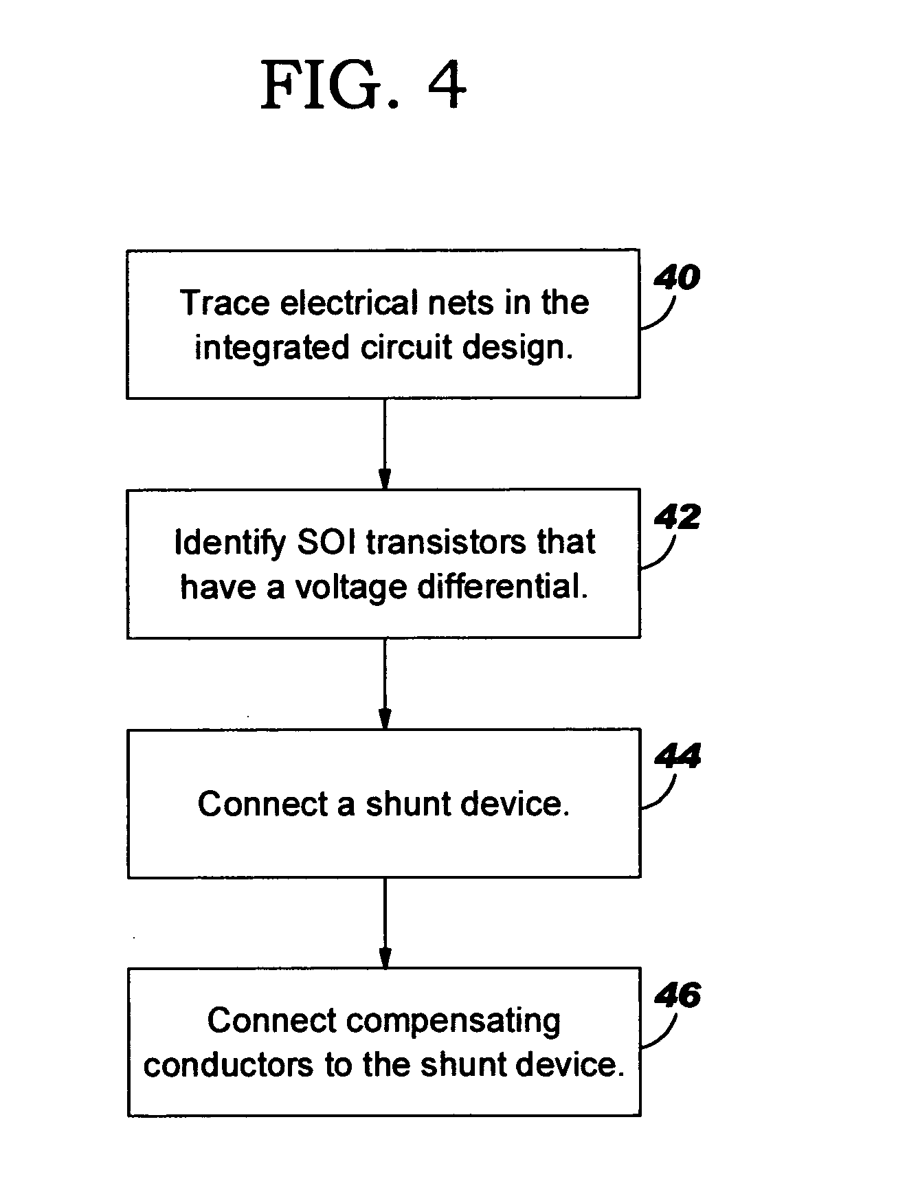
[0016] The present invention and the various features and advantageous details thereof are explained more fully with reference to the nonlimiting embodiments that are illustrated in the accompanying drawings and detailed in the following description. It should be noted that the features illustrated in the drawings are not necessarily drawn to scale. Descriptions of well-known components and processing techniques are omitted so as to not unnecessarily obscure the present invention in detail. The examples used herein are intended merely to facilitate an understanding of ways in which the invention may be practiced and to further enable those of skill in the art to practice the invention. Accordingly, the examples should not be construed as limiting the scope of the invention.

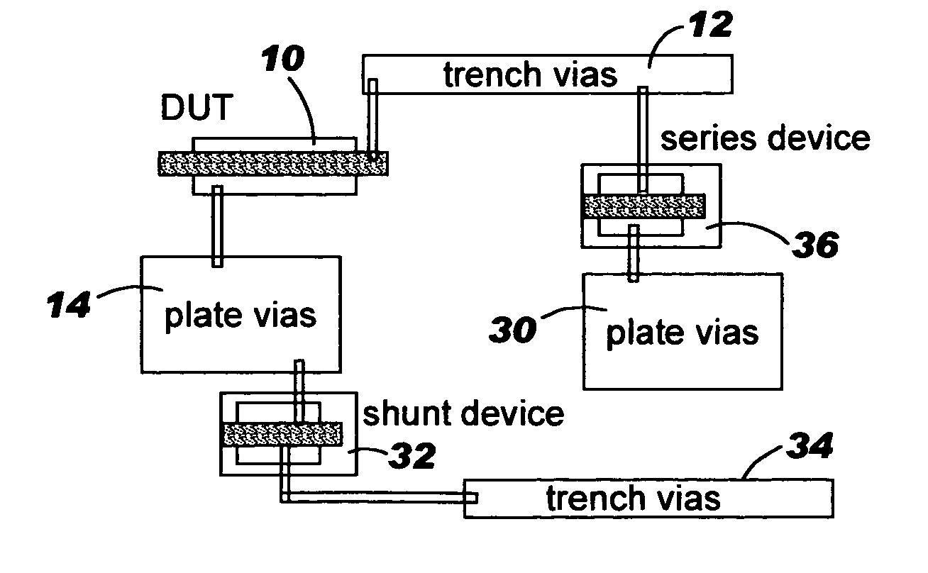
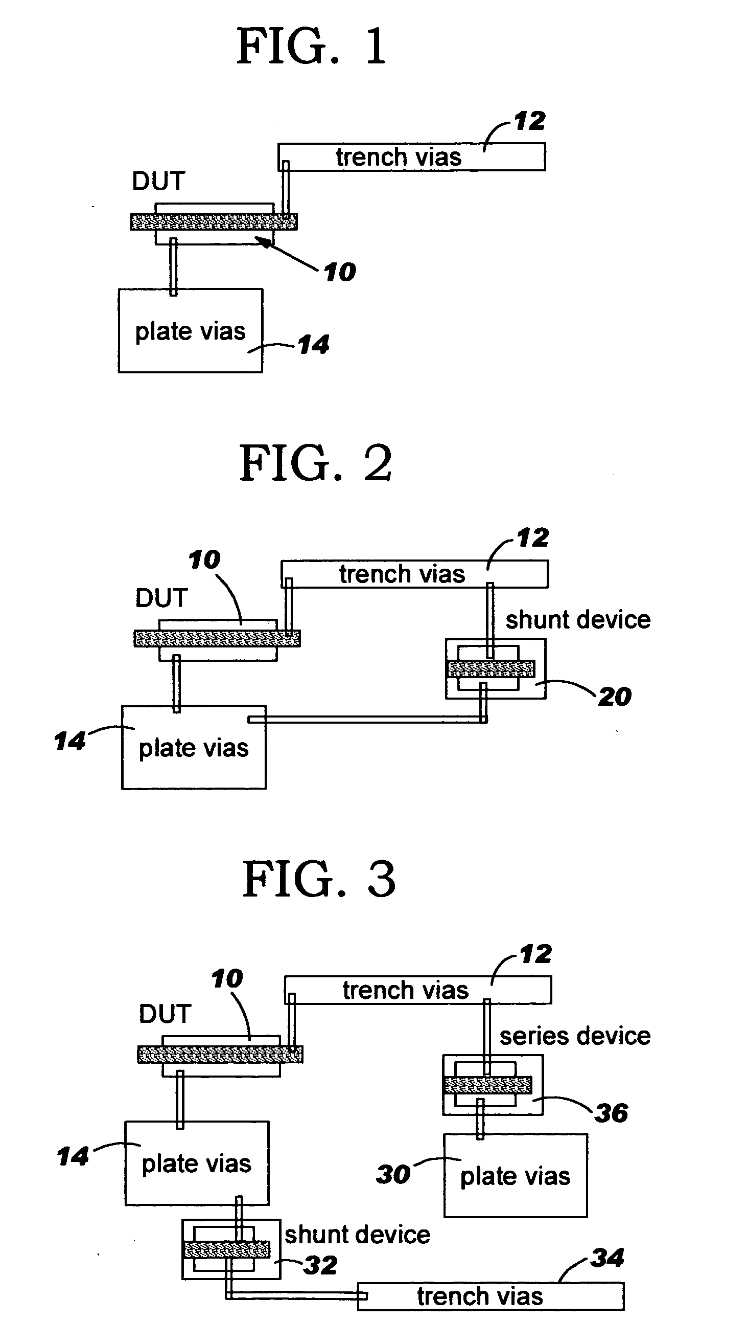
[0017] As mentioned above, even SOI design structures produce the possibility of charging damage. For example, it is possible to create a differential antenna by the arrangement of vias within the metal line. Via...


PUM


Abstract

A method and structure alters an integrated circuit design having silicon over insulator (SOI) transistors. The method/structure prevents damage from charging during processing to the gate of SOI transistors by tracing electrical nets in the integrated circuit design, identifying SOI transistors that have a voltage differential between the source/drain and gate as potentially damaged SOI transistors (based on the tracing of the electrical nets), and connecting a shunt device across the source/drain and the gate of each of the potentially damaged SOI transistors. Alternatively, the method/structure provides for connecting compensating conductors through a series device.

Description

BACKGROUND OF INVENTION [0001] 1. Field of the Invention [0002] The present invention generally relates to protection circuitry and more particularly to a method and structure that includes a shunt device between the source / drain and gate of SOI transistors which may develop a voltage differential between the source / drain and gate during wafer fabrication. The shunt device eliminates the potential for charging damage from processing. [0003] 2. Description of Related Art [0004] One problem that exists when designing integrated circuits with silicon-over-insulator (SOI) transistors relates to the detection of which SOI transistors may be susceptible to charging damage, and to providing protection once such a susceptible device is identified. In SOI it is not possible to “tie down” a floating gate in the traditional sense, such as by adding a diode connection to the substrate or nwell. SOI technologies are inherently less susceptible to charging damage because both the source / drain and...

Claims


Application Information

Patent Timeline
IPC IPC(8): H01L31/0392
CPCH01L27/0251
Inventor BONGES, HENRY A. IIIHARMON, DAVID L.HOOK, TERENCE B.LAI, WING L.
Owner GLOBALFOUNDRIES INC
Why Eureka
Try Eureka