Semiconductor circuit with multiple contact sizes

a technology of contact size and circuit, applied in the direction of semiconductor devices, semiconductor/solid-state device details, electrical apparatus, etc., can solve the problems of increasing the complexity of routing within the built-up layer, affecting the efficiency of the circuit, and consuming power and current normally, so as to reduce the problem of electro-migration, increase the complexity of routing, and reduce the effect of reducing the number of problems

Active Publication Date: 2005-05-05
TEXAS INSTR INC
View PDF17 Cites 7 Cited by
  • Summary
  • Abstract
  • Description
  • Claims
  • Application Information

AI Technical Summary

Benefits of technology

[0006] The invention has several important technical advantages. Various embodiments of the invention may have none, some, or all of these advantages as well as additional advantages. The invention may reduce problems with electro-migration and increased complexity of routing by providing larger contacts (bumps, balls, pins, or columns) for inputs or outputs to the semiconductor circuit which experience higher current than other inputs and outputs. For example, while the invention is not limited to using larger contacts for power and ground inputs and outputs, the use of larger contacts for power and / or ground inputs or outputs may decrease the need to have multiple power and ground inputs and simplify routing. In addition, the use of a larger contact size may provide better mechanical support for the semiconductor circuit when mounted on a printed circuit board either directly (as in a wafer scale application) or indirectly (when used in an array package). Thus, the invention may improve the durability of large die semiconductor circuits while still accommodating a large number of inputs and outputs.

Problems solved by technology

As the size of semiconductor dies increase, in operation, semiconductor circuits employing such dies, normally consume higher amounts of power and current than previous integrated circuits incorporating smaller size dies.
High current flow may cause electro-migration problems either in connection with the contacts for connecting an array package to a printed circuit board or within the contacts for connecting a flip chip die to a substrate within an array package (or directly to a printed circuit board in the case of a wafer scale application).
However, adding inputs and outputs increases the complexity of routing within built up layers both on the package substrate and on the die.
Increasing the complexity of routing leads to more expensive packaging.
Because smaller contacts are more likely to break off when a printed circuit board or semiconductor circuit is subjected to mechanical forces (such as when a circuit board is dropped) large die designs with small contacts are also more fragile than existing designs with larger contacts.

Method used


Image

  • Semiconductor circuit with multiple contact sizes
  • Semiconductor circuit with multiple contact sizes
  • Semiconductor circuit with multiple contact sizes

Examples


second embodiment

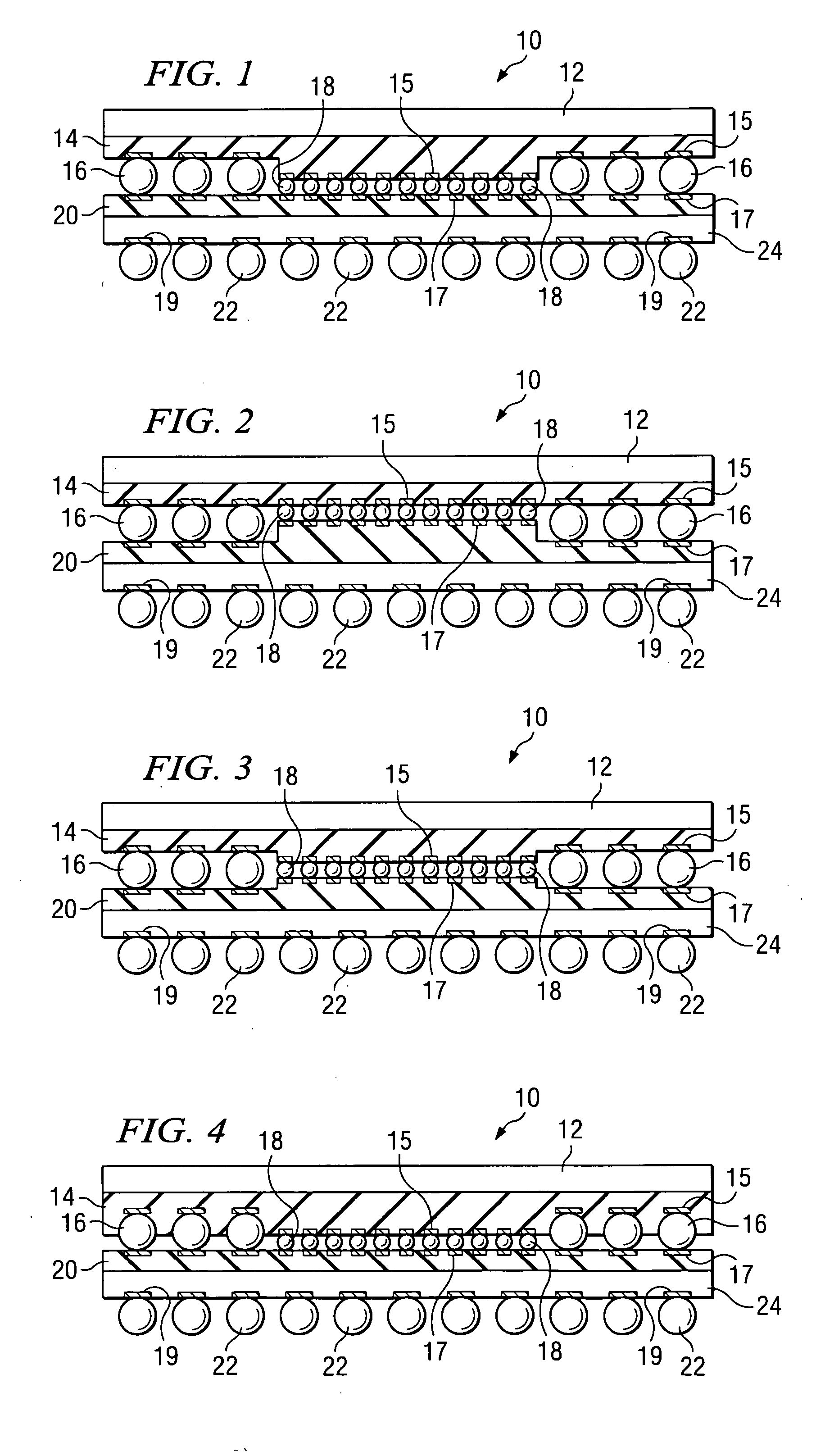
[0024]FIG. 2 illustrates a semiconductor circuit 10 constructed in accordance with the invention. The options discussed in connection with FIG. 1 are equally applicable to the embodiment illustrated in FIG. 2. Thus, the discussion below addresses the differences between the embodiment of FIG. 1 and FIG. 2.

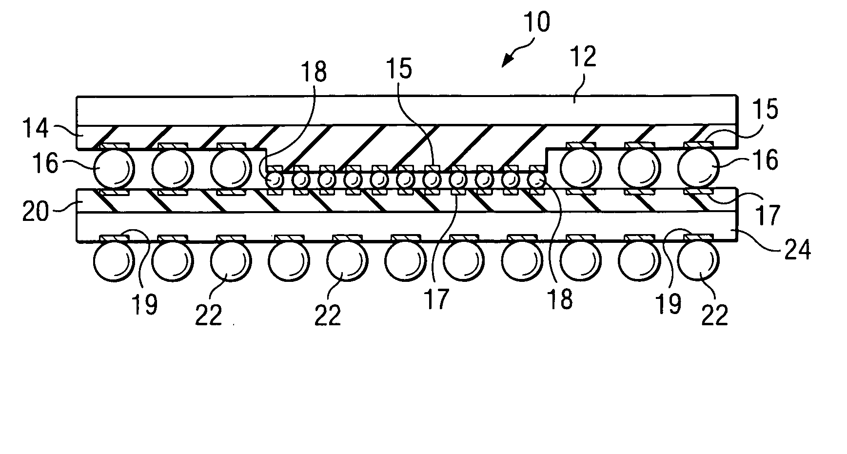
[0025] In FIG. 1, built up layer 14 and die 12 had a non-uniform thickness so as to make the bottom surfaces of large bumps 16 and small bumps 18 substantially coplanar. By making large bumps 16 and small bumps 18 substantially coplanar, die 12 could be attached to package substrate 24 such that die 12 and package substrate 24 were substantially parallel after being bonded to one another.

[0026] In the embodiment of semiconductor circuit 10 illustrated in FIG. 2, however, built up layer 14 is substantially uniform in thickness while the thickness of built up layer 20 on package substrate 24 has been varied such that the top surfaces of large bumps 16 and small bumps 18 (the surface...

third embodiment

[0028]FIG. 3 illustrates a semiconductor circuit 10 constructed in accordance with the teachings of the invention. Again, all of the options discussed in connection with FIG. 1 may apply to the embodiment illustrated in FIG. 3. Thus, the discussion of FIG. 3 concentrates on the differences between the embodiment of FIG. 3 and the previously discussed embodiments of FIGS. 1 and 2.

[0029] In the embodiments of FIG. 1 and 2, either built up layer 14 or built up layer 20 had a substantially uniform thickness while the opposite built up layer 14 or 20 had a varying thickness. In this embodiment, both built up layer 14 and built up layer 20 have a varying thickness. The thickness of both built up layer 14 and built up layer 20 are varied such that die 12 and package substrate 24 are substantially coplanar with one another after they are connected together using large bumps 16 and small bumps 18. Accordingly, both built up layers 14 and 20 may be adjusted to accommodate the varying size of ...


PUM


Abstract

A semiconductor circuit comprising a semiconductor die and a package substrate. In one embodiment, a first plurality of conductive bumps serves as a portion of a conductive path between contacts on the semiconductor die and contacts on the package substrate. A second plurality of conductive bumps serves as a portion of a conductive path between other contacts on the die and contacts on the package substrate. Each of the bumps in the first plurality of conductive bumps is larger than each of the bumps in the second plurality of conductive bumps. In another embodiment, the average size of the first plurality of conductive bumps may be at least 20% larger (or greater) than the average size of the second plurality of bumps.

Description

CROSS REFERENCE TO RELATED APPLICATIONS [0001] This application is related to U.S. application Ser. No. 10 / 453,445 filed on Jun. 3, 2003, by Leland Swanson and Gregory Howard and entitled, “USING SOLDER BALLS OF MULTIPLE SIZES TO COUPLE ONE OR MORE SEMICONDUCTOR STRUCTURES TO AN ELECTRICAL DEVICE.”TECHNICAL FIELD OF THE INVENTION [0002] The present invention relates to semiconductor packaging and more particularly to a semiconductor circuit with multiple contact sizes and a method for manufacturing the same. BACKGROUND OF THE INVENTION [0003] The size of semiconductor die designs continues to increase. As the size of semiconductor dies increase, in operation, semiconductor circuits employing such dies, normally consume higher amounts of power and current than previous integrated circuits incorporating smaller size dies. High current flow may cause electro-migration problems either in connection with the contacts for connecting an array package to a printed circuit board or within th...

Claims


Application Information

Patent Timeline
Patent Type & Authority Applications(United States)
IPC IPC(8): H01L23/31H01L23/485H01L23/498
CPCH01L23/3114H01L23/49816H01L24/10H01L2224/13099H01L2924/14H01L2924/01006H01L24/13H01L2924/01033H01L2924/014H01L2224/1703H01L2924/00H01L2224/13H01L2224/05571H01L2224/05573H01L2924/00014H01L2224/05599
Inventor SWANSON, LELANDHOWARD, GREGORY ERIC
Owner TEXAS INSTR INC
Why Eureka
Try Eureka