Control circuit and reconfigurable logic block
a logic block and control circuit technology, applied in the field of reconfigurable logic blocks, can solve the problems logic circuit reconfiguration, and achieve the effects of large-scale logic circuits and large-scale logic circuits
- Summary
- Abstract
- Description
- Claims
- Application Information
AI Technical Summary
Benefits of technology
Problems solved by technology
Method used
Image
Examples
first embodiment
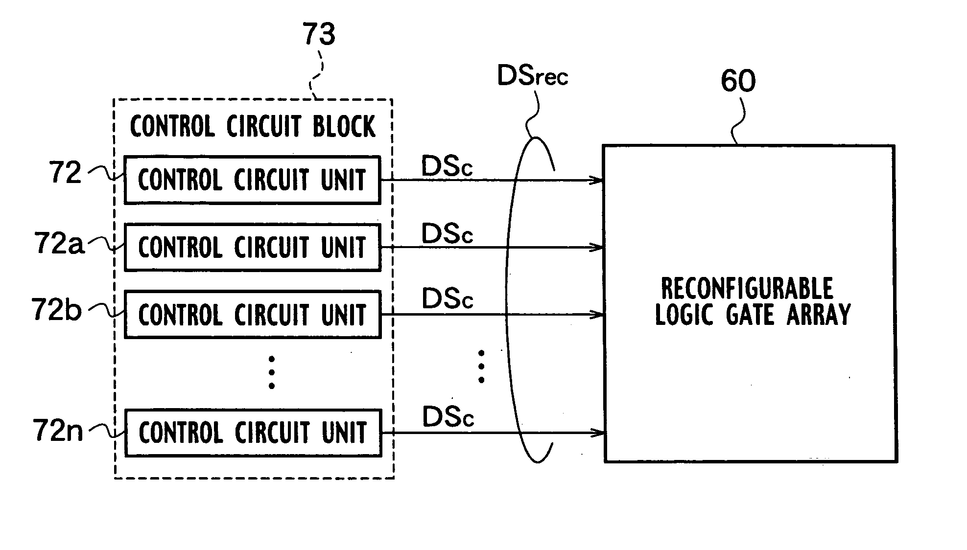
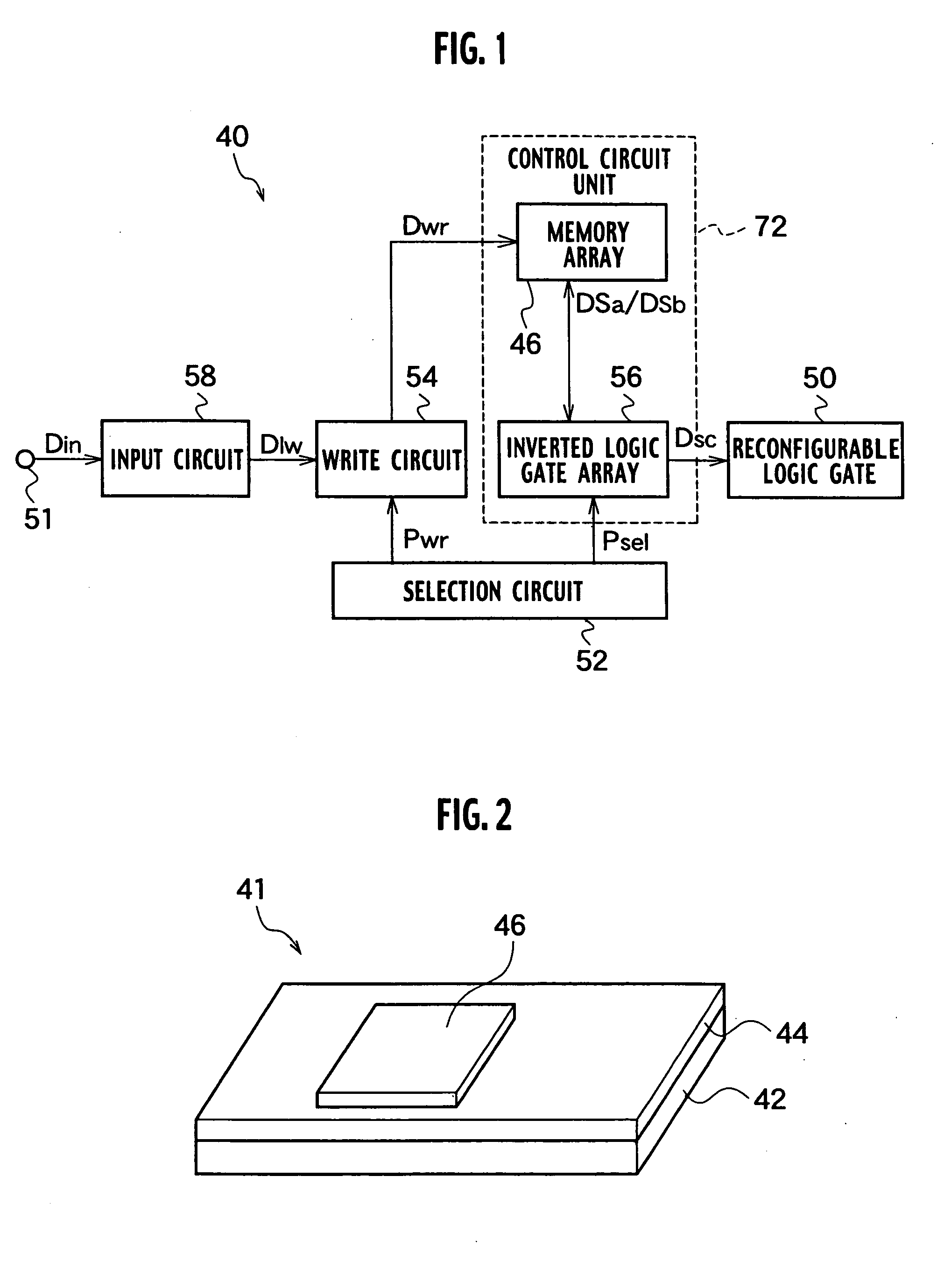
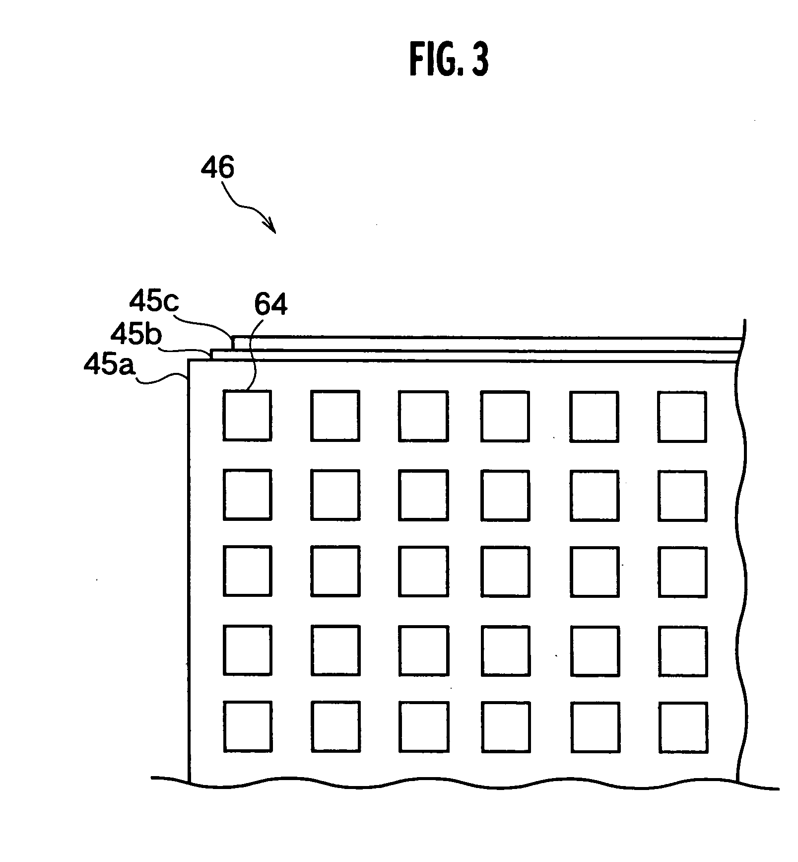
[0034] A reconfigurable logic block 40 according to a first embodiment of the present invention, as shown in FIG. 1, includes an input circuit 58 for acquiring an input signal Din including data used for implementing reconfiguration of logic gates for each of a plurality of logic circuits (hereinafter, referred to as ‘reconfiguration data’) from an input terminal 51 externally connected to, for example, a design system for a logic circuit layout (not shown in the drawing). A write circuit 54 is provided for transmitting a write signal Dwr corresponding to the reconfiguration data by amplifying and converting a circuitry data signal Dlw transmitted from the input circuit 58. A control circuit unit 72 has a memory array 46 storing the reconfiguration data for the plurality of logic circuits in accordance with the write signal Dwr and an inverted logic gate array 56 implementing logical operations based on the stored reconfiguration data by control signals DSa and DSb. The control circ...
second embodiment
[0050] A control circuit 170 of the reconfigurable logic block 40 according to a second embodiment of the present invention, as shown in FIG. 7, includes an inverted logic gate unit 68 providing a reset-set-latch (RS-latch) circuit, and a memory unit 64 inserted in the inverted logic gate unit 68. A first inverted logic gate 76a and a second inverted logic gate 76b in the inverted logic gate unit 68 include a set input terminal S and a reset input terminal R, respectively. A first variable resistive memory 64a is connected between the output terminal Ya of the first inverted logic gate 76a and an input terminal B of the second inverted logic gate 76b. A second variable resistive memory 64b is connected between an input terminal A of the first inverted logic gate 76a and an output terminal Yb of the second inverted logic gate 76b. Output terminals 69a and 69b of the control circuit 170 are connected to the first and second inverted logic gates 76a and 76b, respectively. NAND circuits...
third embodiment
[0060] A reconfigurable logic block 40a according to a third embodiment of the present invention, as shown in FIG. 12, includes the input circuit 58 having an input terminal 51; a control circuit unit 72a having an inverted logic gate array 56a connected to the input circuit 58, and a memory array 46a connected to the inverted logic gate array 56a; a reconfigurable logic gate 50 connected to the inverted logic gate array 56a; and the selection circuit 52 connected to the inverted logic gate array 56a. The input circuit 58 acquires input signals Din including reconfiguration data of logic gates for a plurality of logic circuits from a design system for a logic circuit layout or the like, which is connected to the input terminal 51. The inverted logic gate array 56a, based on a write instruction signal Pwr from the select circuit 52, transmits a circuitry data signal Dlw from the input circuit 58a as a write signal Dwr to the memory array 46a so as to write in the reconfiguration data...
PUM
 Abstract
Description
Claims
Application Information
 - R&D
- Intellectual Property
- Life Sciences
- Materials
- Tech Scout
- Unparalleled Data Quality
- Higher Quality Content
- 60% Fewer Hallucinations
Browse by: Latest US Patents, China's latest patents, Technical Efficacy Thesaurus, Application Domain, Technology Topic, Popular Technical Reports.
© 2025 PatSnap. All rights reserved.Legal|Privacy policy|Modern Slavery Act Transparency Statement|Sitemap|About US| Contact US: help@patsnap.com


