
Slow wave optical waveguide for velocity matched semiconductor modulators

a speed-matched semiconductor and optical waveguide technology, applied in the direction of optical waveguide light guide, instruments, nanotechnology, etc., can solve the problems of difficult design trade-off and down the microwave speed

Active Publication Date: 2005-05-05
NORTHROP GRUMMAN SYST CORP
View PDF18 Cites 3 Cited by
  • Summary
  • Abstract
  • Description
  • Claims
  • Application Information

AI Technical Summary

Benefits of technology

[0012] In accordance with the teachings of the present invention, a PIN electro-optical traveling wave modulator is disclosed that employs optical waveguide structures that can slow the lightwave propagation speed along the direction of interaction. The vertical direction of the waveguide uses conventional refractive index confinement from the epitaxial material layers, while the lateral direction uses periodic structure to provide reflection feedback to the lightwave to allow a “zig-zag” propation ma

Problems solved by technology

This represents a difficult design trade-off between the microwave loss, which requires a wide electrode, and velocity matching, which requires a narrow electrode.
However, this type of approach has design trade-offs, as discussed above, and has only been successful so far, to the best knowledge of the authors, in further slowing down the microwave speed without introducing additional loss.

Method used


Image

  • Slow wave optical waveguide for velocity matched semiconductor modulators
  • Slow wave optical waveguide for velocity matched semiconductor modulators
  • Slow wave optical waveguide for velocity matched semiconductor modulators

Examples


Embodiment Construction

[0016] The following discussion of the preferred embodiments directed to a PIN electro-optical traveling wave modulator is merely exemplary in nature and is in no way intended to limit the invention, or its applications or uses.

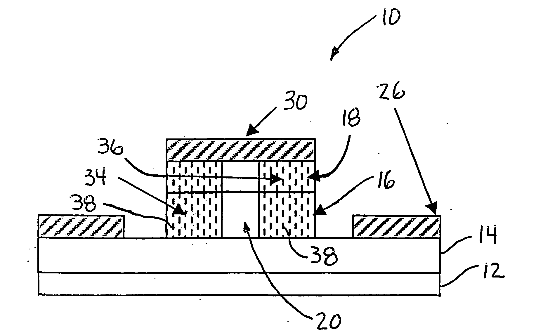
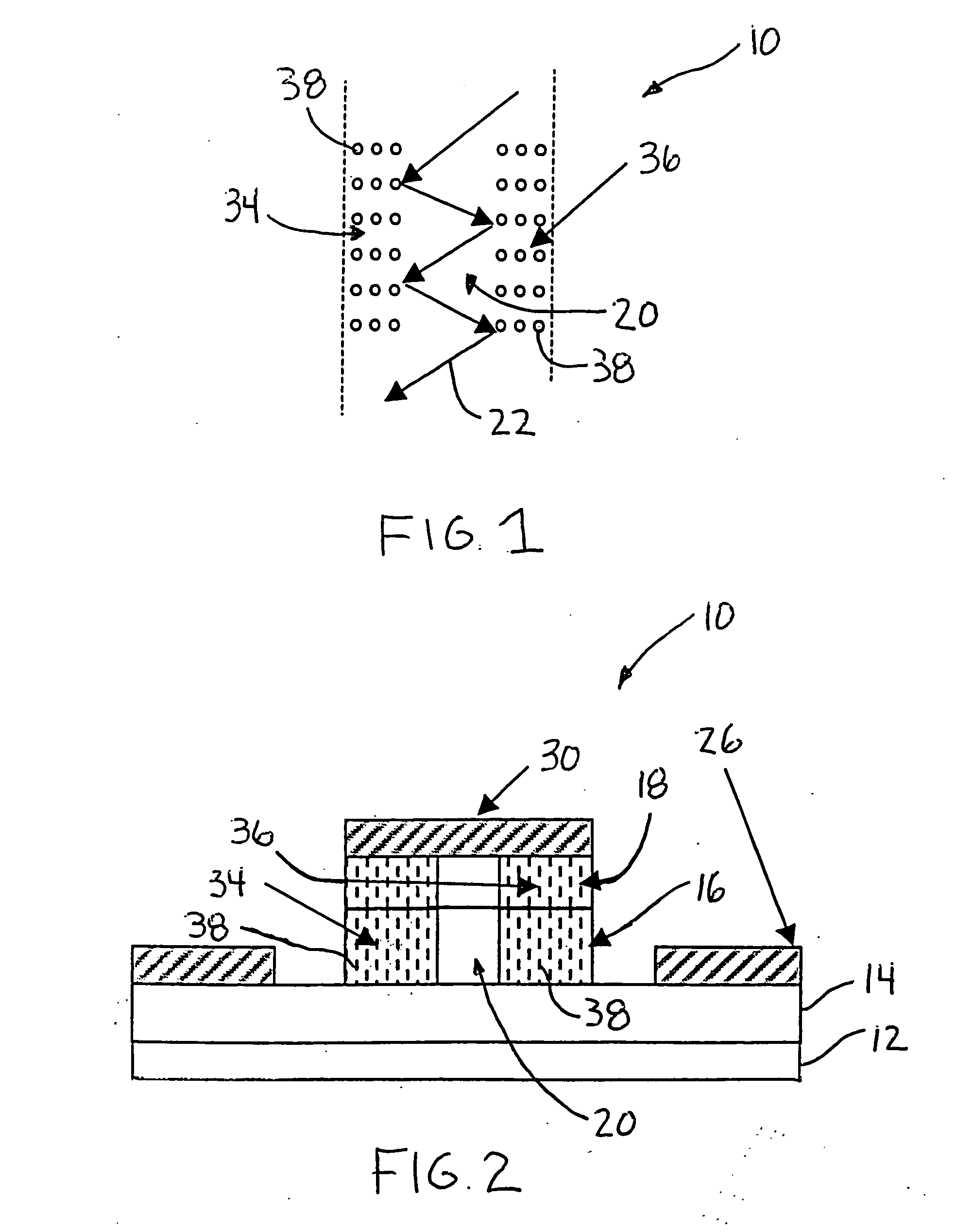
[0017]FIG. 1 is a top view and FIG. 2 is a cross-sectional view of a PIN electro-optical traveling wave modulator 10, according to an embodiment of the present invention. The modulator 10 includes a substrate 12 on which is deposited the various semiconductor device layers that make up the structure of the modulator 10. The semiconductor layers are deposited by a suitable epitaxial deposition process, as would be well understood to those skilled in the art. These semiconductor device layers include an N-type layer 14, an intrinsic layer 16 and a P-type layer 18 configured as shown. As is well known to those skilled in the art, the intrinsic layer 16 contains the device waveguide 20 where an optical wave 22 to be modulated propagates down the waveguide 20. Th...


PUM


Abstract

A PIN electro-optical traveling wave modulator (10) including diffraction gratings (34, 36) positioned at opposing sides of an optical waveguide (20) that act to change the propagation pattern of the waveguide (20). The modulator (10) includes an N-type layer (14), a P-type layer (18) and an intrinsic layer (16) acting as the waveguide (20). A metal electrode (26) is in electrical contact with the N-type layer (14), and a metal electrode (30) is in electrical contact with the P-type layer (18). The electrodes (26, 30) define an RF transmission line. An optical wave (22) propagates along the waveguide (20) and interacts with the gratings (34, 36) which slow the optical wave (22) to match its speed to the speed of the RF wave in the transmission line. In one embodiment, the gratings (34, 36) are 2-D gratings formed by vertical holes (38) in the waveguide (20).

Description

BACKGROUND OF THE INVENTION [0001] 1. Field of the Invention [0002] This invention relates generally to a semiconductor optical modulator and, more particularly, to a semiconductor traveling wave optical modulator that employs diffraction gratings adjacent to the waveguide to slow the optical wave to a speed that matches the speed of the electrical wave in the transmission line. [0003] 2. Discussion of the Related Art [0004] Electro-optical (EO) modulation devices are known in the art that use an electrical signal to frequency modulate an optical signal to impress information on the optical signal. One class of modulation devices of this type include semiconductor quantum well modulators that employ PIN semiconductor device architectures where the optical wave propagates down a waveguide defined within the intrinsic layer in the device. An RF signal is applied to electrodes in contact with the P and N layers to provide the modulation voltage, where the electrodes define an RF transm...

Claims


Application Information

Patent Timeline
IPC IPC(8): G02B6/26G02B6/42G02F1/025G02F1/295
CPCB82Y10/00B82Y20/00G02F2202/32G02F2201/127G02F2201/307G02F1/015G02F1/025
Inventor WANG, WENSHENSCOTT, DAVID CHRISTOPHERKUNKEE, ELIZABETH TWYFORD
Owner NORTHROP GRUMMAN SYST CORP
Learn More