Fabrication method of semiconductor integrated circuit device

a technology of integrated circuit devices and fabrication methods, which is applied in the direction of individual semiconductor device testing, semiconductor/solid-state device testing/measurement, instruments, etc., can solve the problems of not being able to detect, breaking the natural oxide film over and damaging the surface of the test pad itself. , to achieve the effect of reducing the inter-layer insulating film, and reducing the damage to the test pad

Inactive Publication Date: 2005-05-05
RENESAS ELECTRONICS CORP
View PDF3 Cites 20 Cited by
  • Summary
  • Abstract
  • Description
  • Claims
  • Application Information

AI Technical Summary

Benefits of technology

[0035] In the electrical inspection of semiconductor integrated circuit devices, damage...

Problems solved by technology

The wiping of the probes not only breaks the natural oxide film over the surface of the test pads, but also damages the surface of the test pads thems...

Method used


Image

  • Fabrication method of semiconductor integrated circuit device
  • Fabrication method of semiconductor integrated circuit device
  • Fabrication method of semiconductor integrated circuit device

Examples


embodiment 1

(Embodiment 1)

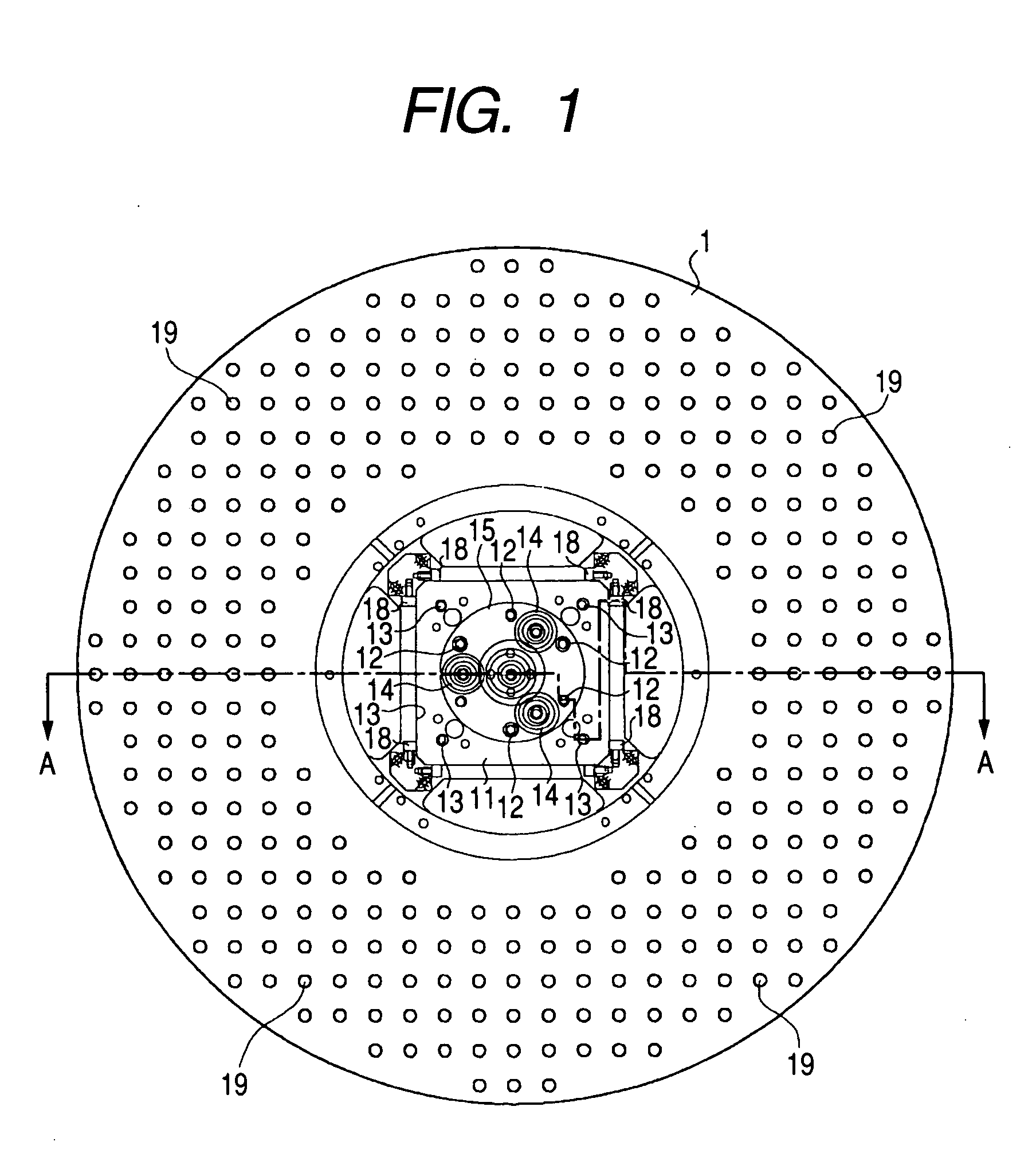
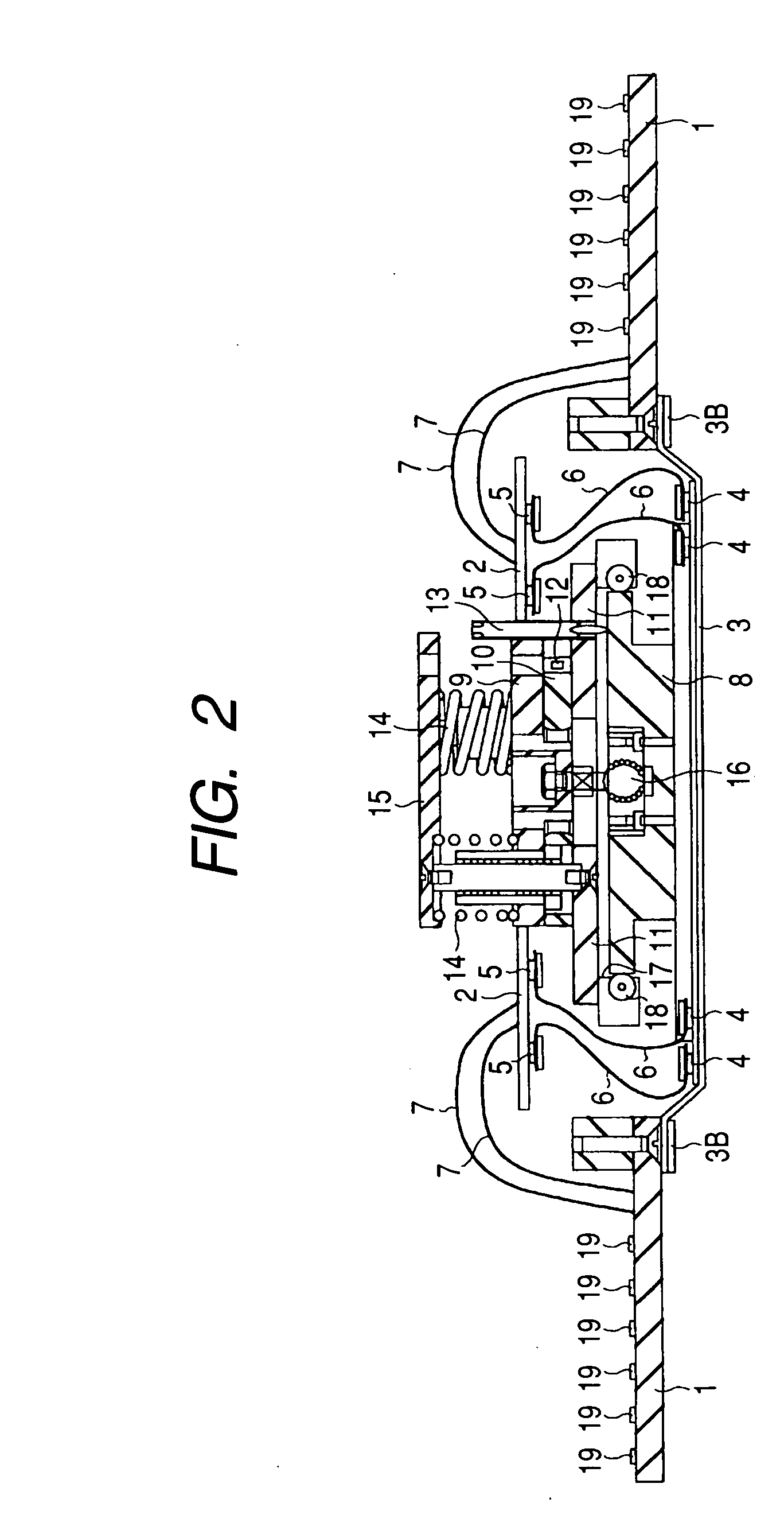
[0092]FIG. 1 is a plan view of a probe card (a first card), which represents Embodiment 1 of the invention, and FIG. 2 shows a section taken along line A-A in FIG. 1.

[0093] As shown in FIG. 1 and FIG. 2, in the probe card according to Embodiment 1, there are formed, for instance, a multi-layered wiring board (third substrate) 1, an auxiliary substrate 2, suppressing means, a thin film probe (first sheet) 3 and so forth. Further, in the probe card of this Embodiment 1, circuits (wirings) are formed in each of the multi-layered wiring board 1, the auxiliary substrate 2 and the thin film probe 3. By forming circuits in each of the multi-layered wiring board 1, the auxiliary substrate 2 and the thin film probe 3, the need to repair the whole probe card in the event of trouble in any one of the multi-layered wiring board 1, the auxiliary substrate 2 and the thin film probe 3 is dispensed with, but only the member in trouble (the multi-layered wiring board 1, the auxiliary ...

embodiment 2

(Embodiment 2)

[0175] Next, an Embodiment 2 of the invention will be described.

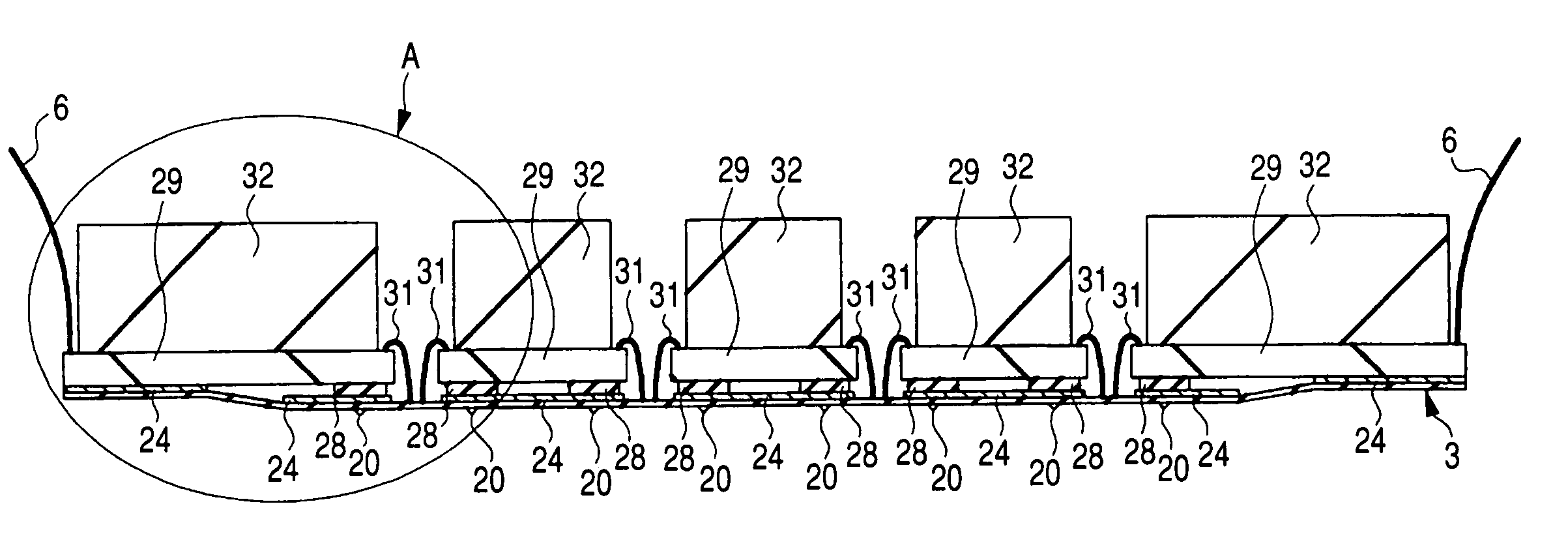
[0176] Among the electrodes (test pads) formed on the main face of the wafer to be inspected, there are some through which relatively large currents flow, including for instance power supply wiring and ground wiring. In this Embodiment 2, as shown in FIG. 28, a plurality of wires 31 are bonded between the bonding pads 21A electrically connected to the probes 20 which come into contact with such electrodes (test pads) and the pads 30. The current capacity between the bonding pads 21A and the pads 30, in which relatively large currents flow, can be enlarged.

[0177] The electrical load on the probes 20 in contact with the electrodes (test pads) in which relatively large currents flow, if formed in the same size as other probes 20, will also be greater. If this electrical load is greater, there may arise such troubles that those probes 20 are heated and welded onto the electrodes (test pads) or are broken. In...

embodiment 3

(Embodiment 3)

[0181] Now, an Embodiment 3 of the invention will be described.

[0182] As shown in FIG. 33, a probe card of this Embodiment 3 is configured by fitting, over the glass epoxy substrate 29 (see also FIG. 4) in the probe card of Embodiment 1, electronic elements 71 electrically connected to a circuit (wiring) formed within the glass epoxy substrate 29. Conceivable examples of the electronic elements 71 in this Embodiment 3 include elements that can constitute relays, capacitors and built-out self test (BOST) circuits (second circuits). The shorter these electronic elements 71 are in electrical distance from the probes 20, the better they will be able to transmit electrical characteristics, such as analog clocks. For this reason, the electronic elements 71 can achieve better electrical characteristics when they are fitted to the glass epoxy substrate 29 than when they are fitted to, for instance, the multi-layered wiring board 1 (see FIG. 1 and FIG. 2).

[0183] Where the ele...


PUM


Abstract

Any damage inflicted on test pads, inter-layer insulating films, semiconductor elements or wiring at the time of electrical inspection of semiconductor integrated circuit devices is to be reduced. Reinforcements having a substantially equal linear expansion ratio (coefficient of thermal expansion) relative to a wafer to be inspected are formed over an upper face of a thin film probe, grooves are cut in the reinforcements above the probes, a first elastomer which is softer than a second elastomer is so arranged as to fill the grooves and overflow the grooves by a prescribed quantity, a glass epoxy substrate, which is a multi-layered wiring board, is fitted over the second elastomer, and pads provided over an upper face of the glass epoxy substrate and bonding pads which are part of wirings belonging to the thin film probe are electrically connected by wires.

Description

CROSS-REFERENCE TO RELATED APPLICATION [0001] The present application claims priority from Japanese patent application No. 2003-372323, filed on Oct. 31, 2003, the content of which is hereby incorporated by reference into this application. BACKGROUND OF THE INVENTION [0002] The present invention relates to a technique for use in the fabrication of semiconductor integrated circuit devices, and, more particularly, to a technique that can be effectively applied to electrical inspection of semiconductor integrated circuits in a semiconductor wafer state. [0003] For instance, there is a known technique for use in forming contact terminals, lead-out wiring and the like of an inspection apparatus for use in probing semiconductor integrated circuits in a wafer state (see Patent Reference 1 and Patent Reference 2, for example). By this method, a mold for shaping contact terminals is prepared by anisotropic etching of a silicon wafer, for example, and contact terminals, lead-out wiring and th...

Claims


Application Information

Patent Timeline
IPC IPC(8): G01R3/00G01R1/073G01R31/28H01L21/66
CPCG01R1/07307G01R3/00H01L2924/1306H01L2924/10253H01L2224/73265H01L2924/01322H01L2924/01045H01L2924/01024H01L2924/01019H01L2924/01006H01L2924/01005H01L2924/30107H01L2924/19041H01L2924/01082H01L2924/01079H01L2924/01078H01L2924/01033H01L2924/01029H01L2924/0102H01L2924/01013H01L2224/92247H01L2224/4903H01L2224/4824H01L2224/48227G01R31/2889H01L24/32H01L2224/32225H01L2224/48091H01L2924/00014H01L2924/00H01L2924/3512H01L2924/12042H01L2924/14G01R1/0735H01L22/00
Inventor HASEBE, AKIONARIZUKA, YASUNORIMOTOYAMA, YASUHIROSHOJI, TERUO
Owner RENESAS ELECTRONICS CORP
Why Eureka
Try Eureka