Packaging apparatus for optical interconnection on optical printed circuit board

Active Publication Date: 2005-05-12
SAMSUNG ELECTRONICS CO LTD
View PDF10 Cites 75 Cited by
  • Summary
  • Abstract
  • Description
  • Claims
  • Application Information

AI Technical Summary

Benefits of technology

[0011] The present invention has been made in view of the above problems, and it is an object of the present invention t

Problems solved by technology

In the simplest structure, in which the optically active element is directly flip-bonded to the printed circuit board, the optically active element has a relatively small size compared to the diameter of the solder balls and the size of the metal pads on the printed circuit board, manufactured by a conventional process, thus causing difficulty in precisely integrating the optically active element onto the printed circuit board.
In the BGA structure, since the BGA substrate is manufactu

Method used


Image

  • Packaging apparatus for optical interconnection on optical printed circuit board
  • Packaging apparatus for optical interconnection on optical printed circuit board
  • Packaging apparatus for optical interconnection on optical printed circuit board

Examples


Embodiment Construction

[0026] Preferred embodiments of the present invention are described below in detail with reference to the annexed drawings. In the following description of the present invention, detailed description of known functions and configurations is omitted for clarity of presentation.

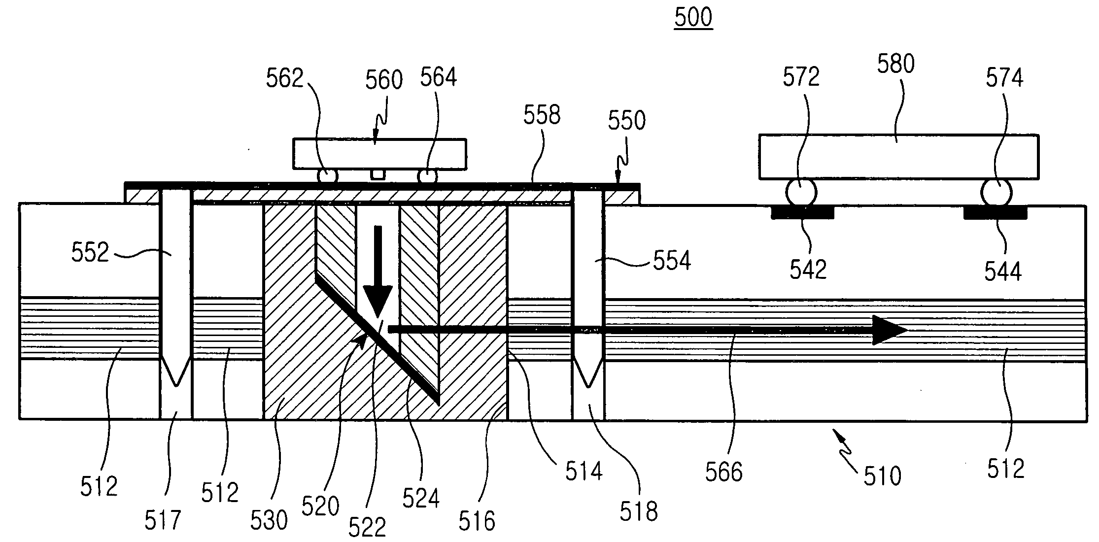
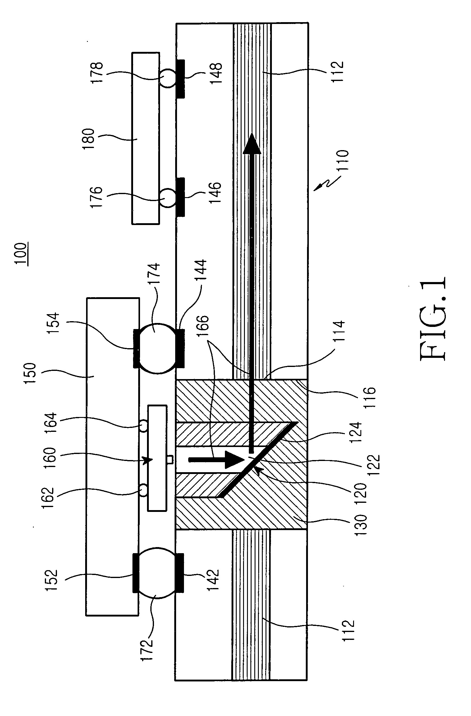
[0027]FIG. 1 is a cross-sectional view of a packaging apparatus for optical interconnection on an optical PCB in accordance with a first preferred embodiment of the present invention. The apparatus 100 comprises a printed circuit board 110, an optical interconnection block 120, a package substrate 150, a surface emitting element 160, and a transmitting chip 180.

[0028] The printed circuit board 110 includes an optical waveguide 112 therein, and an optical via hole 116 contacting the optical waveguide. The optical waveguide 112 has a stacked structure in the printed circuit board 110, and serves as a route by which an optical signal is transmitted. The printed circuit board 110 includes a plurality of metal pad...


PUM


Abstract

A packaging apparatus for optical interconnection on an optical PCB includes a first substrate with a via hole formed therethrough and in which an optical waveguide is formed, an optical interconnection block having a reflective plane on its lower end inserted into the via hole, a second substrate flip-bonded to an upper surface of the first substrate, and an optically active element flip-bonded to a lower surface of the second substrate and aligned for optical communication.

Description

CLAIM OF PRIORITY [0001] This application claims priority to an application entitled “PACKAGING APPARATUS FOR OPTICAL INTERCONNECTION ON OPTICAL PRINTED CIRCUIT BOARD,” filed in the Korean Intellectual Property Office on Nov. 11, 2003 and assigned Serial No. 2003-79543, the contents of which are hereby incorporated by reference. BACKGROUND OF THE INVENTION [0002] 1. Field of the Invention [0003] The present invention relates to a packaging apparatus for optical interconnection, and more particularly to a packaging apparatus for optical interconnection on an optical PCB, in which an optically active element (such as a semiconductor laser, a photo diode, etc.) is mounted on a printed circuit board (hereinafter, referred to as an “optical PCB”) provided with an optical waveguide. [0004] 2. Description of the Related Art [0005] In the simplest structure of packaging apparatus for optical interconnection on an optical PCB, which is well known to those skilled in the art, metal pads and s...

Claims


Application Information

Patent Timeline
IPC IPC(8): G02B6/12G02B6/42H05K1/02
CPCG02B6/42H05K1/0274G02B6/4214G02B6/12
Inventor KIM, DONG-SUPARK, HYO-HOONCHO, HAN-SEORHO, BYUNG-SUPJUNG, SUN-TAE
Owner SAMSUNG ELECTRONICS CO LTD
Why Eureka
Try Eureka