Transmitting type secondary electron surface and electron tube

a technology of secondary electron and surface, applied in the direction of electron multiplier details, image-conversion/image-amplification tubes, tubes with screens, etc., can solve the problem that the emission efficiency of secondary electrons of the second electron emitter has not been practical, and achieve the effect of preventing improving the emission efficiency of secondary electrons according to the primary electron, and high efficiency

Inactive Publication Date: 2005-05-19
HAMAMATSU PHOTONICS KK
View PDF12 Cites 13 Cited by
  • Summary
  • Abstract
  • Description
  • Claims
  • Application Information

AI Technical Summary

Benefits of technology

[0009] The present invention has been made to solve the aforementioned problems. It is an object of the present invention to provide a transmission secondary electron emitter which can emit the secondary electrons efficiently for the incidence of the primary electrons, and an electron tube using the same.
[0011] According to the above construction, the transmission secondary electron emitter has a transmission construction in which one surface of the secondary electron emitting layer is the surface of the incidence, and the other surface is the surface of the emission. Thereby the construction prevents the change in the surface condition of the surface of the emission by the incidence of the primary electrons, and the decrease in the emission efficiency of the secondary electrons can be prevented. The secondary electron emitting layer is made of diamond or a material containing diamond as a main component, and thereby the emission efficiency of the secondary electrons according to the primary electrons can be improved. The voltage applying means forms the electric field in the secondary electron emitting layer. Thereby the secondary electrons reach the surface of the emission easily, and the secondary electrons can be emitted with high efficiency.
[0012] The electron tube according to the present invention comprises: the above transmission secondary electron emitter; an electron source for emitting the primary electrons to the transmission secondary electron emitter; an anode for collecting secondary electrons emitted from the transmission secondary electron emitter; and an envelope for accommodating the transmission secondary electron emitter, the electron source, and the anode. The use of the transmission secondary electron emitter for the electron tube provides an electron tube which can efficiently obtain the secondary electrons from the incidence of the primary electrons.

Problems solved by technology

However, the above transmission secondary electron emitter has not had the practical emission efficiency of secondary electrons.

Method used


Image

  • Transmitting type secondary electron surface and electron tube
  • Transmitting type secondary electron surface and electron tube
  • Transmitting type secondary electron surface and electron tube

Examples


first embodiment

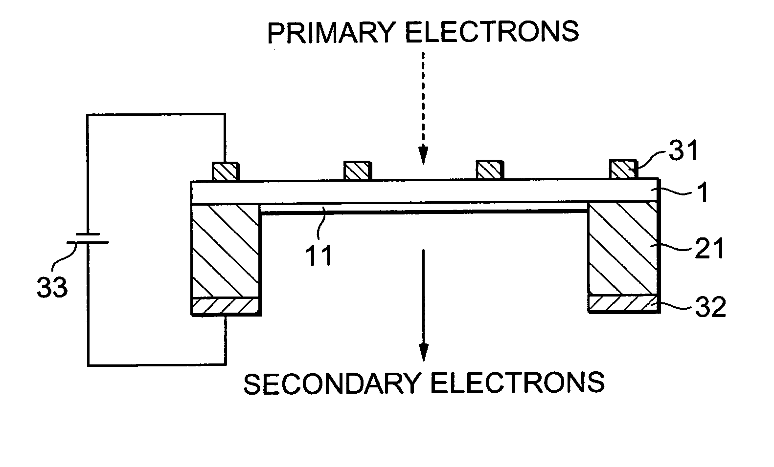
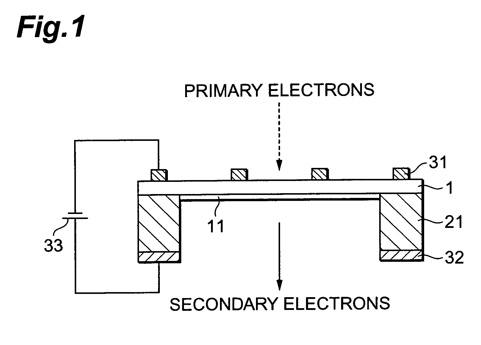
[0026]FIG. 1 is a side cross-sectional view illustrating the construction of a transmission secondary electron emitter according to the present invention. FIG. 2 is a perspective view of the transmission secondary electron emitter shown in FIG. 1.

[0027] A transmission secondary electron emitter illustrated in FIG. 1 comprises a secondary electron emitting layer 1, a supporting frame 21, a first electrode 31 and a second electrode 32. In the transmission secondary electron emitter, secondary electrons are generated in the secondary electron emitting layer 1 by an incidence of primary electrons, and secondary electrons are emitted outside. The transmission secondary electron emitter has a transmission type construction. One surface (an upper surface in FIG. 1) of the secondary electron emitting layer 1 is the surface of the incidence for making the primary electrons incident thereon, and the other surface (a lower surface in FIG. 1) of the side opposite thereto is the surface of the e...

second embodiment

[0052]FIG. 4 is a side cross-sectional view illustrating the construction of the transmission secondary electron emitter according to the

[0053] The transmission secondary electron emitter shown in FIG. 4 comprises the secondary electron emitting layer 1, the active layer 11, the supporting frame 21, a first electrode film 31a, an auxiliary electrode 34 and the second electrode 32. Of these, the constructions of the secondary electron emitting layer 1, the active layer 11, the supporting frame 21 and the second electrode 32 are identical to those of the transmission secondary electron emitter shown in FIG. 1.

[0054] The first electrode film 31a is formed in the film state on the surface of the incidence of the secondary electron emitting layer 1. The first electrode film 31a is very thinly formed (the thickness of about 30 to 150 Å) such that the secondary electrons generated in the secondary electron emitting layer 1 are not absorbed by the first electrode film 31a. The auxiliary el...

third embodiment

[0059]FIG. 5 is a side cross-sectional view illustrating the construction of the transmission secondary electron emitter according to the

[0060] The transmission secondary electron emitter shown in FIG. 5 comprises the secondary electron emitting layer 1, the active layer 11, a supporting frame 22, a first electrode 35 and a second electrode 36. Of these, the constructions of the secondary electron emitting layer 1 and the active layer 11 are identical to those of the transmission secondary electron emitter shown in FIG. 1.

[0061] The supporting frame 22 is a supporting means for reinforcing the mechanical strength of the secondary electron emitting layer 1 formed thinly. The supporting frame 22 is arranged on the outer edge part of the surface of the incidence of the secondary electron emitting layer 1.

[0062] The first electrode 35 formed on the surface of the incidence of the secondary electron emitting layer 1 is an electrode of an incident surface side. In this embodiment, the f...


PUM


Abstract

The transmission secondary electron emitter according to the present invention comprises a secondary electron emitting layer 1 made of diamond or a material containing diamond as a main component, a supporting frame 21 reinforcing the mechanical strength of the secondary electron emitting layer 1, a first electrode 31 formed on the surface of incidence of the secondary electron emitting layer 1, and a second electrode 32 formed on the surface of emission of the secondary electron emitting layer 1. A voltage is applied between the surfaces of the incidence and the emission of the secondary electron emitting layer 1 to form an electric field in the secondary electron emitting layer 1. When the incidence of primary electrons into the secondary electron emitting layer 1 generates secondary electrons in the secondary electron emitting layer 1, the secondary electrons are accelerated in the direction to the surface of the emission by the electric field formed in the secondary electron emitting layer 1, and emitted out of the transmission secondary electron emitter. Therefore, a transmission secondary electron emitter capable of efficiently emitting the secondary electrons by the incidence of the primary electrons, and an electron tube using the same can be achieved.

Description

FIELD OF THE ART [0001] The present invention relates to a transmission secondary electron emitter emitting secondary electrons generated by primary electrons made incident, and an electron tube provided with the transmission secondary electron emitter. BACKGROUND ART [0002] Attention has been recently focused on a secondary electron emitter which is used for an electron tube and uses diamond. The reason for this is that the diamond has negative electron affinity, and the diamond has high secondary electron-emission efficiency. One example is reported in “Thin Solid Films 253(1994) p 151.” In the example, the diamond is used as a material for a reflection type secondary electron emitter of which the surface of emission for emitting secondary electrons is the same as the surface of incidence for making primary electrons incident thereon. That is, in the secondary electron emitter, a polycrystalline diamond thin film of which the surface is terminated with hydrogen is formed on a subs...

Claims


Application Information

Patent Timeline
Patent Type & Authority Applications(United States)
IPC IPC(8): H01J1/35H01J1/32H01J29/02H01J29/48H01J31/12H01J31/50H01J43/22
CPCH01J1/32H01J29/023H01J43/22H01J31/50H01J31/506H01J29/482
Inventor NIIGAKI, MINORUUCHIYAMA, SHOICHIKAN, HIROFUMI
Owner HAMAMATSU PHOTONICS KK
Why Eureka
Try Eureka