Light-emitting diode

a light-emitting diode and light-emitting element technology, applied in the direction of lasers, semiconductor lasers, solid-state devices, etc., can solve the problems of reducing luminous efficiency, reducing the mobility of the diode, and reducing the luminous efficiency of the diode, so as to reduce the defect density and reduce the luminous efficiency. , the effect of high mobility

Inactive Publication Date: 2006-11-23
HOYA CORP
View PDF4 Cites 56 Cited by
  • Summary
  • Abstract
  • Description
  • Claims
  • Application Information

AI Technical Summary

Benefits of technology

[0021] According to the present invention, since a dopant is not introduced into a light-emitting layer, crystal growth can be achieved with low defect density, and a light-emitting diode capable of performing efficient light emission can be provided which is free from a reduction in luminous efficiency due to the dopant and from emission of light of unnecessary wavelengths due to the dopant. Further, since it is possible to use diamond, a group II-VI compound semiconductor, a group III-V compound semiconductor or the like as the light-emitting layer, mobility is high, thereby allowing not only sufficient emission intensity to be obtained, but also an emission wavelength to be selected in a wide range from ultraviolet light to infrared light. Moreover, since a p-type semiconductor and an n-type semiconductor are not needed, a semiconductor difficult to convert into a p type or an n type can be used for the light-emitting layer to manufacture the light-emitting diode. Still further, since not only a monocrystalline but also polycrystalline or amorphous substrate can be employed as the substrate, a glass substrate, a plastic substrate and the like can be used, and moreover, a transparent substrate can be used, so that the present invention enables manufacture of a large-area light-emitting device.
[0022] An embodiment of the present invention will hereinafter be described in detail with reference to the drawings.
[0024]FIG. 1 is a diagram showing a structure of a vertical light-emitting diode which is one embodiment of the present invention. In the light-emitting element of the present invention, an n-electrode 12 is formed on a substrate 11, and an ambipolar inorganic semiconductor 13 which is a light-emitting layer is stacked on the n-electrode 12, and a p-electrode 14 is further stacked on the ambipolar inorganic semiconductor

Problems solved by technology

Thus, this dopant causes deformation, defects and the like in a semiconductor crystalline structure, and these will be quenching centers to reduce luminous efficiency and induce emission of light of unnecessary wavelengths.
Further, a conventional p-n junction type light-emitting diode is limited in a range of semic

Method used


Image

  • Light-emitting diode
  • Light-emitting diode
  • Light-emitting diode

Examples


example 1

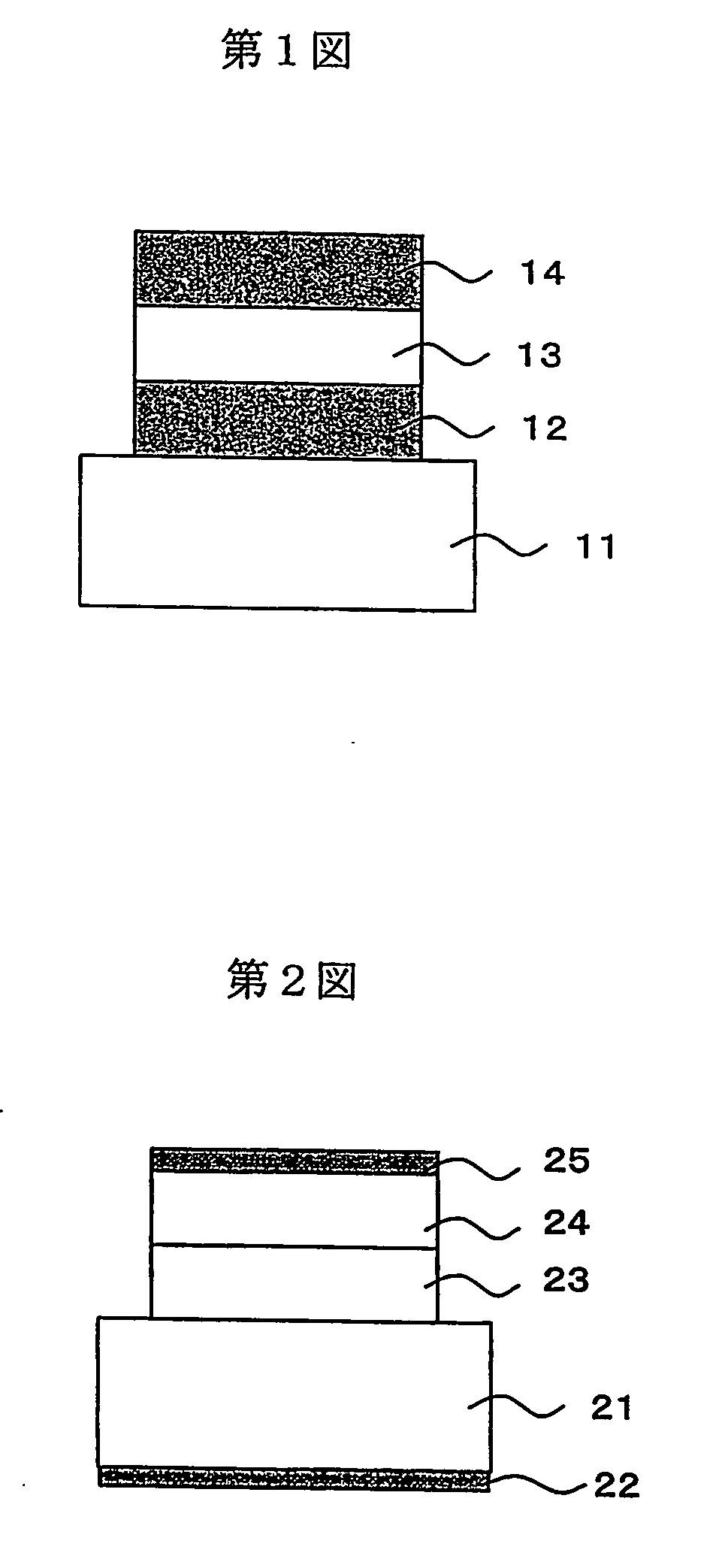
[0119] ZnSe was selected as an ambipolar inorganic semiconductor forming a light-emitting layer. A GaAs (100) monocrystalline wafer (carrier density: 1×10¹⁸ / cm3) doped n-type was immersed in a so-called piranha solution (mixed solution of H2, O2, H2OS4) to remove an oxide layer on a surface thereof. This was quickly introduced as a substrate for film formation into a molecular beam epitaxy (MBE) vacuum device for film formation (manufactured by Eikoh Engineering, ultimate vacuum: 5×10⁻¹⁰ Torr), and fixed thereto. Then, a temperature of the substrate was raised to 500° C., and it was confirmed by looking a reflection high energy electron diffraction image (RHEED) that a clean and flat surface was exposed. Further, the substrate temperature was dropped to 400° C., and a molecular beam of each component was emitted from a Zn cell and an Se cell and applied to the GaAs (100) substrate, thereby forming a ZnSe thin film at 2 μmt.

[0120] Next, carrier mobility in the thin film was measured...

example 2

[0122] As in Example 1, an n-GaAs (100) monocrystalline wafer was immersed in a piranha solution, and introduced and fixed in an MBE vacuum device for film formation. A temperature was raised to 500° C., and it was confirmed by looking a reflection high energy electron diffraction image (RHEED) that a clean and flat surface was exposed. Then, the substrate temperature was dropped to 400° C., and a molecular beam of each component was emitted from a Zn cell, an Se cell and an Al cell, and applied to the n-GaAs (100) substrate, thereby forming a film of an n-type ZnSe doped with Al at 2 μmt. In other words, an n-electrode having an n-GaAs / n-ZnSe structure was formed. Next, a ZnSe layer is stacked on this layer at 200 nmt to produce a light-emitting layer. Further, a molecular beam of an N atom in a radical state was applied onto the substrate together with the molecular beams of Zn and Se by use of an ion source manufactured by Oxford Applied Research Corporation, and a film of p-ZnSe...

example 3

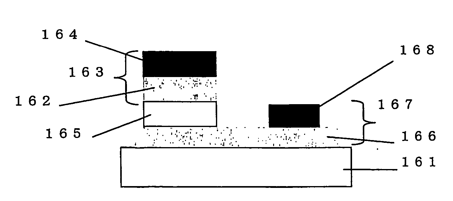
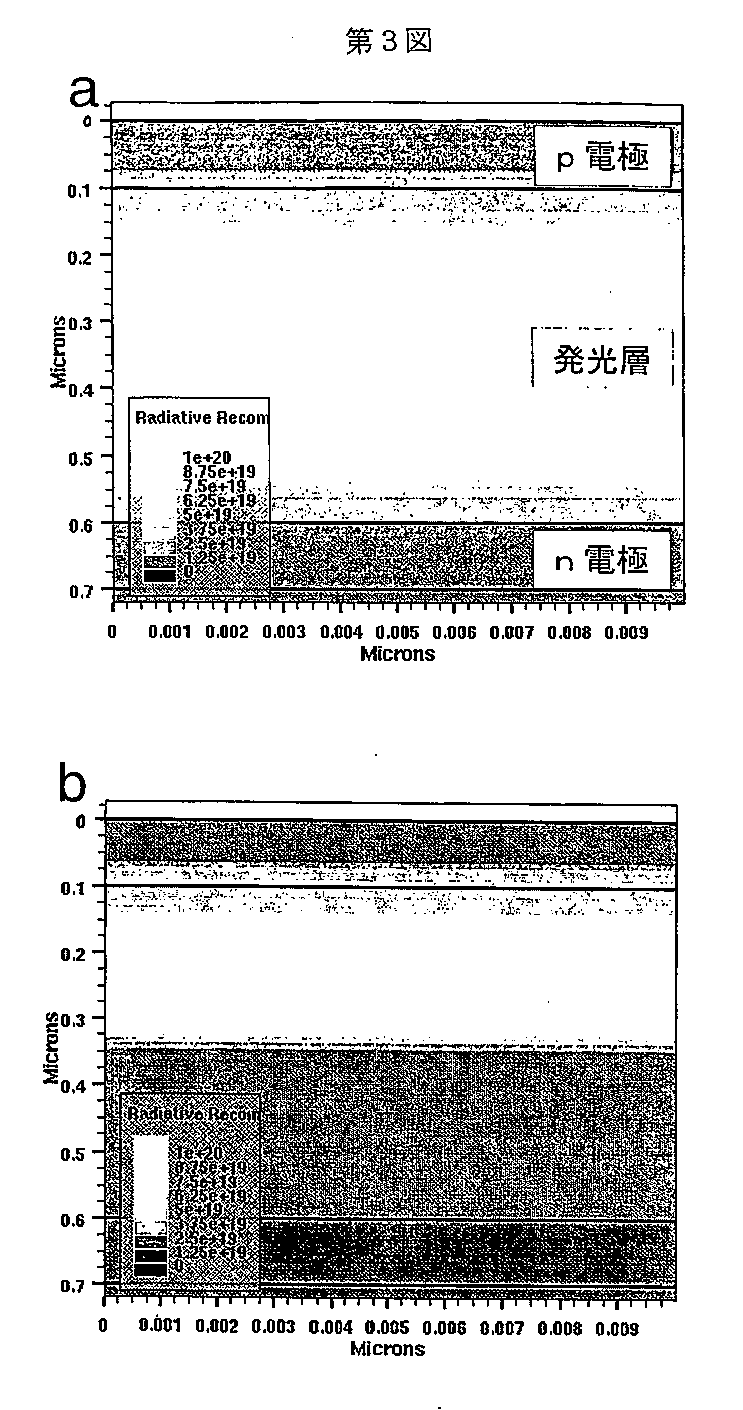
[0133] In Example 2, a stacking order was changed in the following manner. Example 3 will be described with reference to FIG. 10. A p-ZnSe film 136 doped with N was formed at 2 μm on a non-doped p-GaAs (100) substrate 131. Next, part of the p-ZnSe substrate 136 was covered with a mask, and a ZnSe layer 135 was stacked at 200 nm on the remainder, thereby producing a light-emitting layer. Moreover, after an Mg film 132 was deposited on the light-emitting layer 135, the Mg film 132 was covered with an Au film 134, and an n-electrode 133 was thus produced as an Mg / Au laminated film. Next, the mask covering a surface of p-ZnSe was removed, and a Pd film 138 was vapor-deposited on the surface, and then an Au film 139 was further deposited thereon, thereby creating a p-ZnSe / Pd / Au structure as a p-electrode 137. When a voltage of 10 V was applied across the electrodes, an emission spectrum similar to that of curve (a) in FIG. 8 was obtained.

[0134] In addition, when a Cl-doped n-ZnSe / Mg / Au ...


PUM


Abstract

A light-emitting diode with high luminous efficiency is provided which is free from deformation or defects of a crystal caused by a dopant. The light-emitting diode emits no light of unnecessary wavelengths and has a wide selection of emission wavelengths. The light-emitting diode comprises a light-emitting layer made of an ambipolar semiconductor containing no dopant, and an electron implanting electrode, that is, an n-electrode and a hole implanting electrode, that is, a p-electrode joined to the light-emitting layer.

Description

FIELD OF THE INVENTION [0001] The present invention relates to a two-terminal-type light-emitting element using a semiconductor, that is, a light-emitting diode. BACKGROUND ART [0002] Light-emitting elements using semiconductors are widely used for displays and light sources, and have recently started to be used as illumination to replace incandescent light bulbs and fluorescent lights. A light-emitting diode is one of such light-emitting elements. [0003] The light-emitting diode is composed of a p-type inorganic semiconductor layer and an n-type inorganic semiconductor layer joined to each other at a p-n junction, an example of a prior art document is “A Guide to Optoelectronics”, written by Kenya Goto, page 75, Ohm Corporation, 1981. The p-type semiconductor and the n-type semiconductor are formed by diffusing a p-type or n-type dopant into a semiconductor. The p-type dopant produces holes in the semiconductor, while the n-type dopant produces electrons in the semiconductor. [0004...

Claims


Application Information

Patent Timeline
IPC IPC(8): H01L33/00H01L33/02H01S5/30H01S5/323
CPCH01L33/025H01S5/32341H01S5/3027H01S5/3018
Inventor KAWAZOE, HIROSHIORITA, MASAHIROYANAGITA, HIROAKIKOBAYASHI, SATOSHI
Owner HOYA CORP
Why Eureka
Try Eureka