Display device and imaging method

a display device and image technology, applied in the field of display devices having an image capture function and an imaging method, can solve the problems of poor display quality, large noise of obtained image, and inability to correctly subject the gamma adjustment, and achieve the effect of excellent display quality and little nois

Inactive Publication Date: 2005-05-19
JAPAN DISPLAY CENTRAL CO LTD
View PDF9 Cites 24 Cited by
  • Summary
  • Abstract
  • Description
  • Claims
  • Application Information

AI Technical Summary

Benefits of technology

[0012] In order to solve the above-described problem, an object of the present invention is to provide a display device having an image capture function with an excellent display quality and with little noises.

Problems solved by technology

According to this method, however, the picked-up image finally obtained is not correctly subjected to a gamma adjustment, and therefore, has poor display quality.
There is also a risk that the obtained image has much noise, depending on characteristics of the photoelectric conversion element.
There is also a risk that a setting of an image capture condition is complex.

Method used


Image

  • Display device and imaging method
  • Display device and imaging method
  • Display device and imaging method

Examples


Embodiment Construction

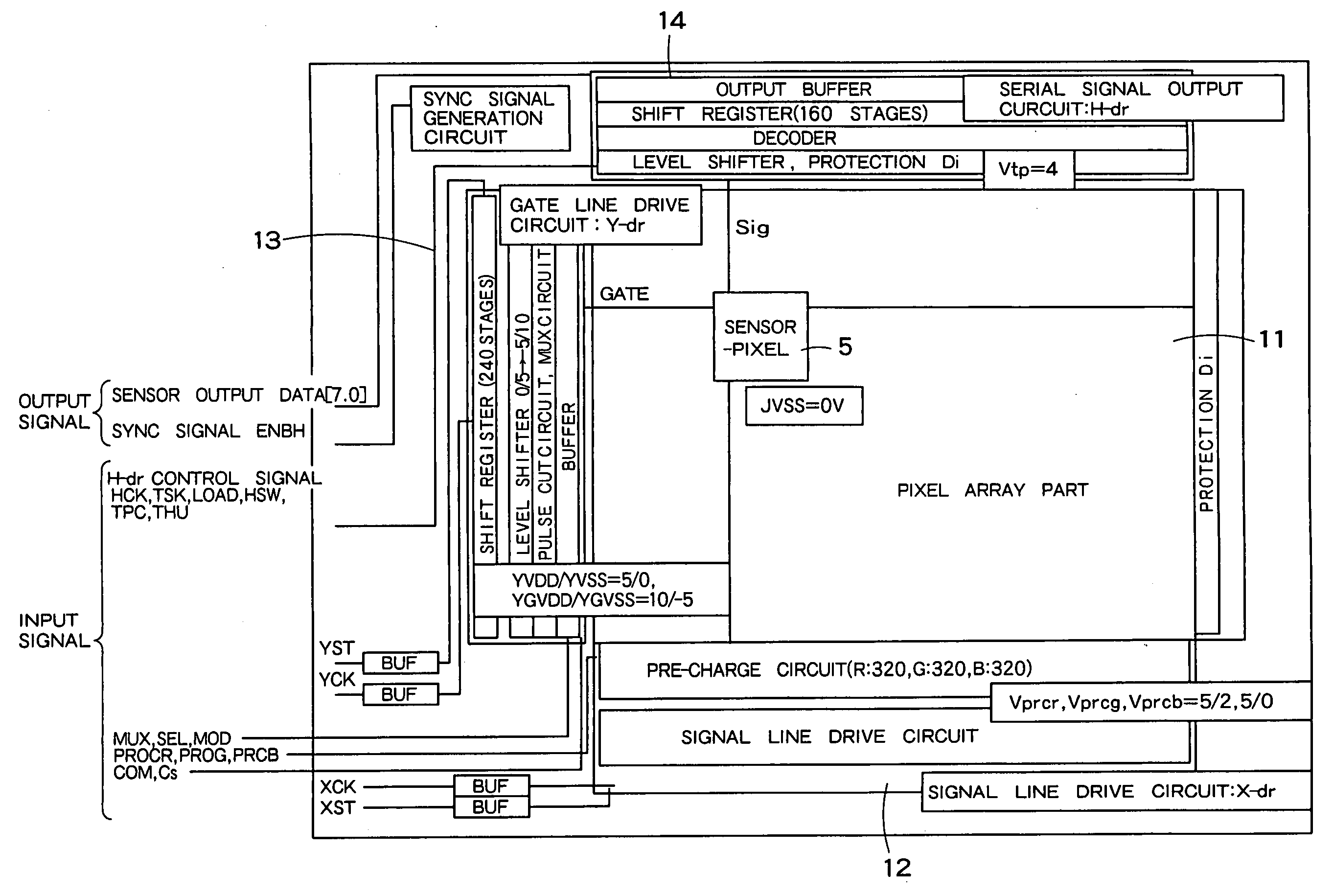
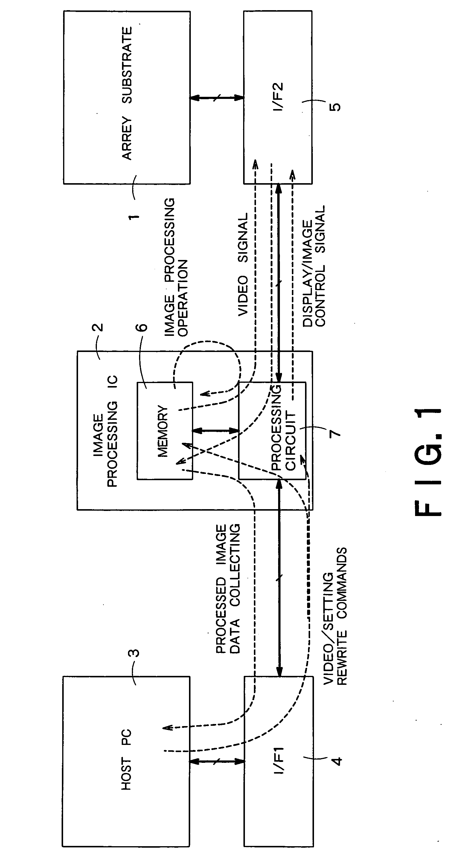
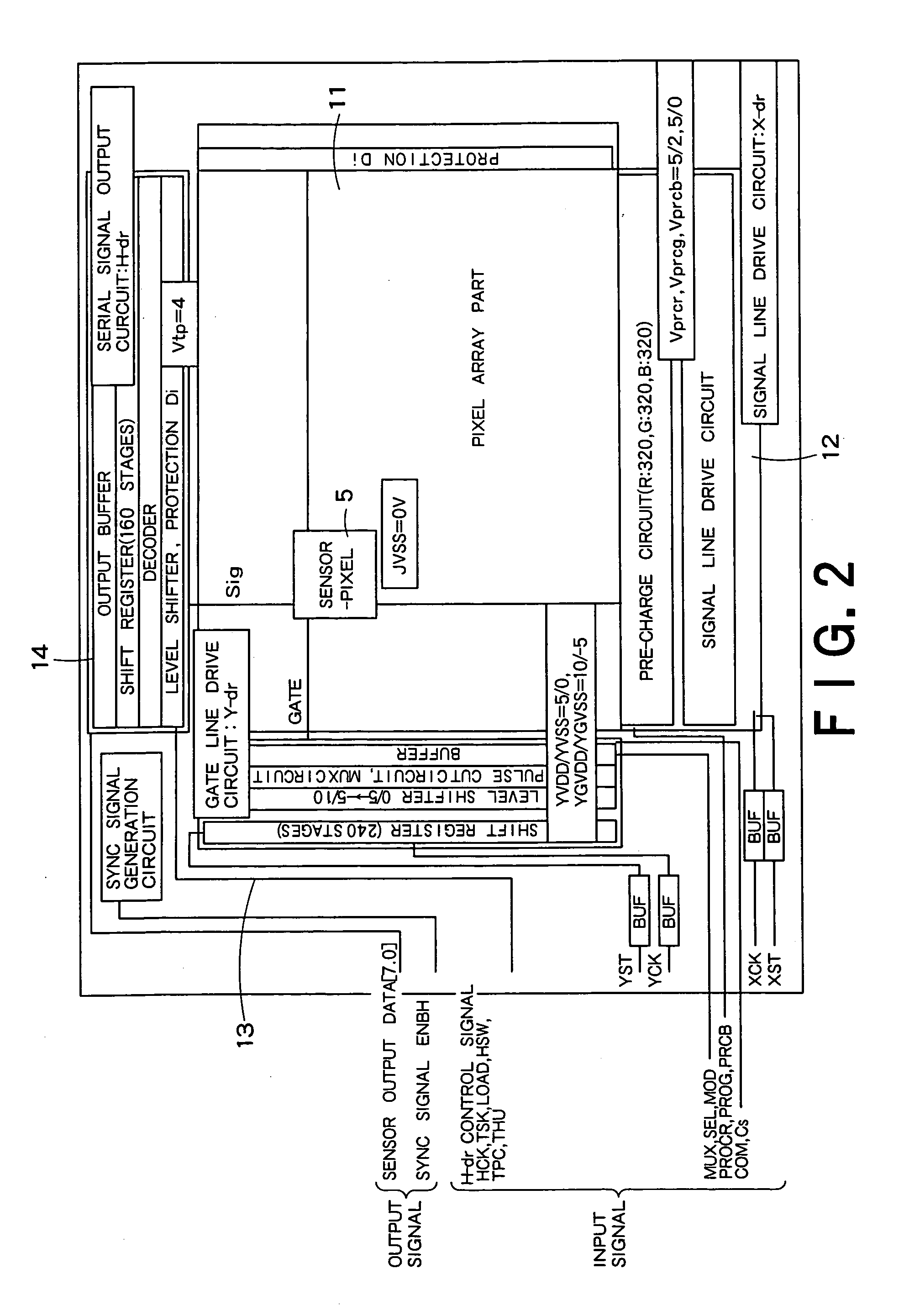
[0053] Hereafter, a display device and an imaging method according to the present invention will be described more specifically with reference to the drawings. FIG. 1 is a block diagram showing a schematic configuration of a display device according to one embodiment of the present invention. The display device shown in FIG. 1 includes an array substrate 1, an image processing IC (integrated circuit) 2, a host PC (personal computer) 3, an interface (I / F1) 4 that exchanges signals between the host PC 3 and the image processing IC 2, and an interface (I / F2) 5 that exchanges signals between the array substrate 1 and the image processing IC 2.

[0054] The image processing IC 2 can be mounted on the array substrate 1, or can be mounted on another separate from the array substrate 1. The image processing IC 2 can have any package such as an ASIC (an LSI for a specific application), and an FPGA (a programmable LSI). The image processing IC 2 has a memory 6 and a processing circuit 7. For th...


PUM

PropertyMeasurementUnit
temperatureaaaaaaaaaa
display colorsaaaaaaaaaa

Abstract

A display device has a pixel array part having display elements provided inside of pixels formed in vicinity of cross points of signal lines and scanning lines aligned in matrix form; image capture circuits provided corresponding to the display elements, each including an optical sensor which picks up image at prescribed range of an imaging subject; and an image capture processing unit which generates ultimate image capture data based on result of having picked up images a plurality of times while changing image capture condition except for display color, with respect to each of M kinds of display colors.

Description

CROSS REFERENCE TO RELATED APPLICATIONS [0001] This application claims benefit of priority under 35USC§119 to Japanese Patent Application No. 2003-387039, filed on Nov. 17, 2003, the entire contents of which are incorporated by reference herein. BACKGROUND OF THE INVENTION [0002] 1. Field of the Invention [0003] The present invention relates to a display device having an image capture function, and an imaging method. [0004] 2. Related Art [0005] A liquid crystal display device has an array substrate on which signal lines, scanning lines, and pixel TFTs (thin film transistors) are disposed, and drive circuits that drives the signal lines and the scanning lines. Based on recent advancement and development of integrated circuit technology, a process technique of forming a part of the drive circuits on the array substrate is in practical use. With this technique, the total liquid crystal display device can be made light, thin and compact, to enable the display device to be widely used f...

Claims


Application Information

Patent Timeline
Patent Type & Authority Applications(United States)
IPC IPC(8): G06T1/00G02F1/133G06F1/16G06F3/041G06F3/048G09G3/20G09G3/36G09G5/00H04N1/46H04N1/60H04N5/335H04N5/365H04N5/369H04N9/04H04N9/30
CPCG06F3/0488G06F3/0412G06F3/042G02F1/133G09G3/36
Inventor NAKAMURA, TAKASHIYOSHIDA, MASAHIROISHIKAWA, MIYUKI
Owner JAPAN DISPLAY CENTRAL CO LTD
Why Eureka
Try Eureka