Conditioning of a reaction chamber

a reaction chamber and reaction chamber technology, applied in the direction of electrical equipment, decorative surface effects, decorative arts, etc., can solve the problems of changing and failing the electrical characteristics of the device, increasing the critical dimension of the integrated circuit,

Inactive Publication Date: 2005-05-19
MICRON TECH INC
View PDF6 Cites 4 Cited by
  • Summary
  • Abstract
  • Description
  • Claims
  • Application Information

AI Technical Summary

Benefits of technology

[0011] As batches of semiconductor wafers are processed, the standard deviation of the critical dimensions of the features patterned on the semiconductor wafers may increase. This variance in the critical dimensions of the integrated circuits formed on semiconductor wafers is also referred to as critical dimension d

Problems solved by technology

Disadvantageously, errors in the patterning and removal process may affect the critical dimensions of the integrated circuit, and may result in changes and failures in the electrical characteristics

Method used


Image

  • Conditioning of a reaction chamber
  • Conditioning of a reaction chamber
  • Conditioning of a reaction chamber

Examples


Embodiment Construction

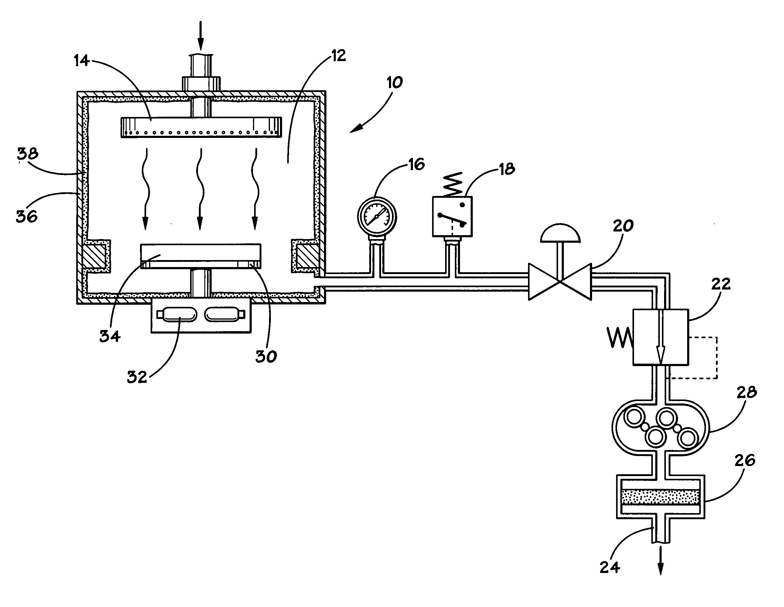
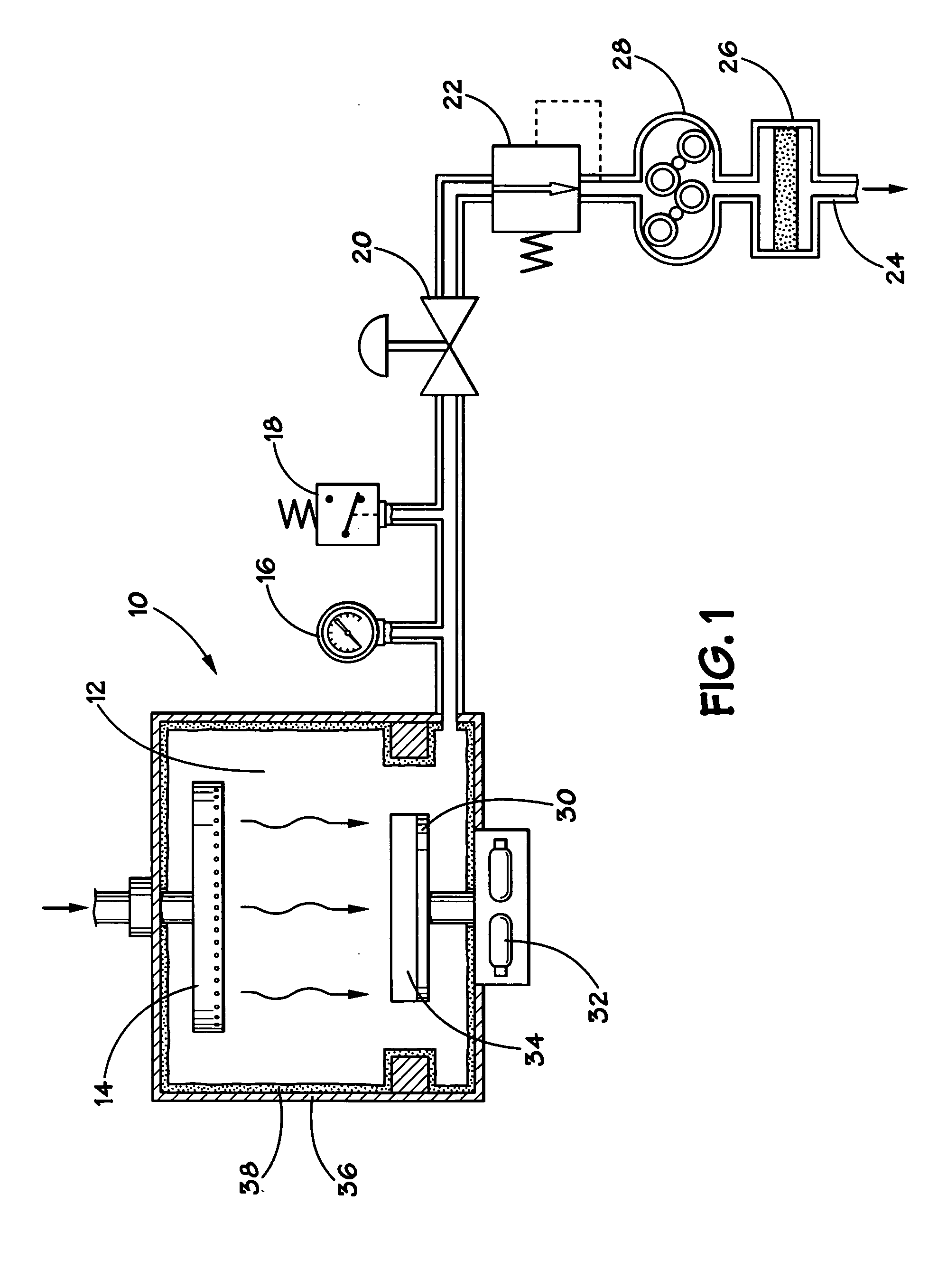
[0017] One or more specific embodiments of the present invention will be described below. In an effort to provide a concise description of these embodiments, not all features of an actual implementation are described in the specification. It should be appreciated that in the development of any such actual implementation, as in any engineering or design project, numerous implementation-specific decisions must be made to achieve the developers' specific goals, such as compliance with system-related and business-related constraints, which may vary from one implementation to another. Moreover, it should be appreciated that such a development effort might be complex and time consuming, but would nevertheless be a routine undertaking of design, fabrication, and manufacture for those of ordinary skill having the benefit of this disclosure.

[0018] Through comparison of various processing techniques, it has been found that the presence of polymer in a reactor chamber in which semiconductor w...


PUM

PropertyMeasurementUnit
Temperatureaaaaaaaaaa
Magnetic fieldaaaaaaaaaa

Abstract

A method is provided for forming polymer on an interior surface of a reaction chamber. A polymer-forming gas is introduced into the chamber and the environment is regulated to form the polymer on the interior surface of the chamber. Methods for the manufacture of integrated circuits, electronic devices, and electronic systems, are also provided.

Description

BACKGROUND OF THE INVENTION [0001] 1. Field Of The Invention [0002] This present invention relates generally to the field of integrated circuit manufacturing technology and, more specifically, to reducing the standard deviation of the critical dimensions of integrated circuit structures. [0003] 2. Description of The Related Art [0004] This section is intended to introduce the reader to aspects of the art that may be related to various aspects of the present invention, which are described and / or claimed below. This discussion is believed to be helpful in providing the reader with background information to facilitate a better understanding of the various aspects of the present invention. Accordingly, it should be understood that these statements are to be read in this light, and not as admissions of prior art. [0005] In the manufacturing of integrated circuits, numerous microelectronic circuits are simultaneously manufactured on a semiconductor substrate. These substrates are usually ...

Claims


Application Information

Patent Timeline
IPC IPC(8): B44C1/22H01L21/302H01L21/311
CPCH01L21/31138
Inventor POLINSKY, WILLIAM A.CRANE, BILLGONZALES, JOHN C.OTT, STEVEN
Owner MICRON TECH INC
Why Eureka
Try Eureka