

Highly reliable stack type semiconductor package
- Summary
- Abstract
- Description
- Claims
- Application Information
AI Technical Summary
Benefits of technology
Problems solved by technology
Method used
Image

Examples
first embodiment
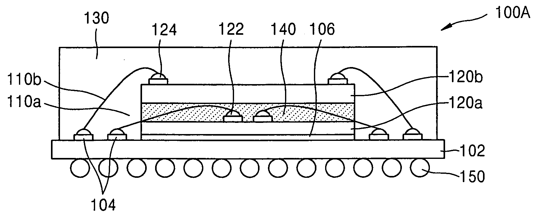
[0035]FIG. 3 is a sectional view of a stack type semiconductor package 100A according to the present invention.
[0036] Referring to FIG. 3, a stack type semiconductor package 100A includes a basis frame 102, which is formed of a lead frame and a substrate, a first semiconductor chip 120a, first wires 110a, a second die adhesive 140, a second semiconductor chip 120b, second wires 110b, and a sealing portion 130. The first semiconductor chip 120a is mounted on the basis frame 102 using a first die adhesive 106. The first wires 110a connect bond pads 122, which are formed near the center of the first semiconductor chip 120a, with contact units 104 on the basis frame 102. The second die adhesive 140 is formed on the first semiconductor chip 120a on which the first wires 110a are formed, and the second die adhesive 140 is expanded to the edges of the first semiconductor chip 120a. Here, the bulk modulus of the second die adhesive 140 is greater than 1 GPa. The second semiconductor chip 12...
second embodiment
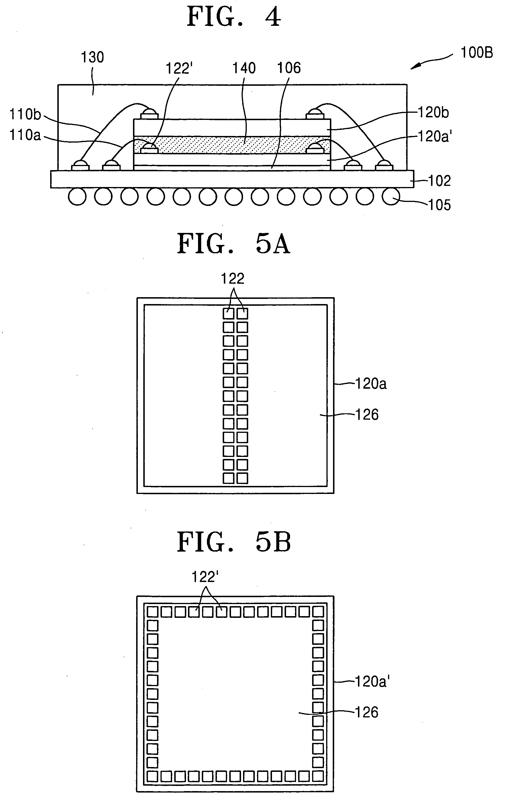
[0042]FIG. 4 is a sectional view of a stack type semiconductor package 100B according to the present invention.
[0043] Referring to FIG. 4, the semiconductor package 100B is similar to the semiconductor package 100A, except that bond pads 122′ are formed at the edges of a first semiconductor chip 120a′. Accordingly, further description of the semiconductor package 100B will be omitted.
[0044]FIGS. 5A and 5B are plan views of the semiconductor chips used in the semiconductor packages 100A and 100B of FIGS. 3 and 4, respectively.
[0045] Referring to FIG. 5A, the semiconductor chip 120a includes the bond pads 122 disposed near the center. In FIG. 5B, the semiconductor chip 120a′ includes the bond pads 122′ near the edges. Both the semiconductor chips 120a and 120a′ include an active region on which circuits are formed.
third embodiment
[0046]FIG. 6 is a sectional view of a stack type semiconductor package 100C according to the present invention.
[0047] Referring to FIG. 6, the semiconductor package 100C additionally includes a heat sink 160, which is not included in the semiconductor package 100B, below the first die adhesive 106 in order to efficiently extract heat from the first and second semiconductor chips 120a′ and 120b. The material included in, the location of, and the shape of the heat sink 160 can be varied.
PUM
 Abstract
Description
Claims
Application Information