Programmable phase-locked loop

a phase-locked loop and loop technology, applied in the direction of phase difference detection, automatic control of pulses, angle demodulation, etc., can solve the problem of end user of integrated circuits without flexibility to change the frequency range of the pll

Active Publication Date: 2005-05-26
AVAGO TECH INT SALES PTE LTD
View PDF13 Cites 26 Cited by
  • Summary
  • Abstract
  • Description
  • Claims
  • Application Information

AI Technical Summary

Problems solved by technology

This leaves the end user of the integrated circuit wi...

Method used


Image

  • Programmable phase-locked loop
  • Programmable phase-locked loop
  • Programmable phase-locked loop

Examples


Embodiment Construction

[0014] As semiconductor technologies advance and become more complex, the costs associated with manufacturing each of the masks that are used to fabricate an integrated circuit have increased significantly. The degree to which each mask is customized for a particular application further increases the costs associated with manufacturing the mask and increases its design time. Therefore, it is desired to reduce the level of customization of certain logic functions while still providing the customer with wide ranges of operating characteristics.

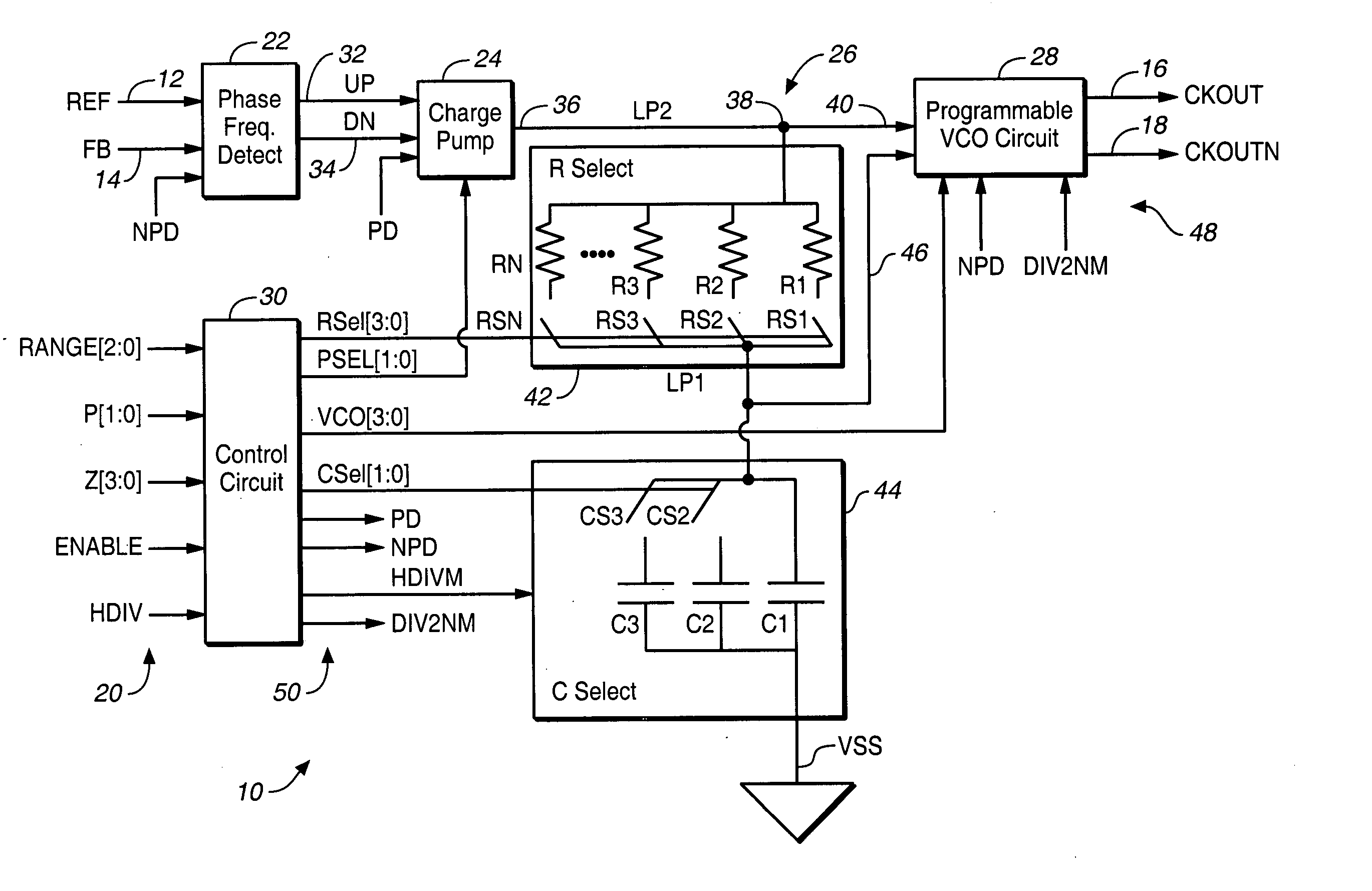
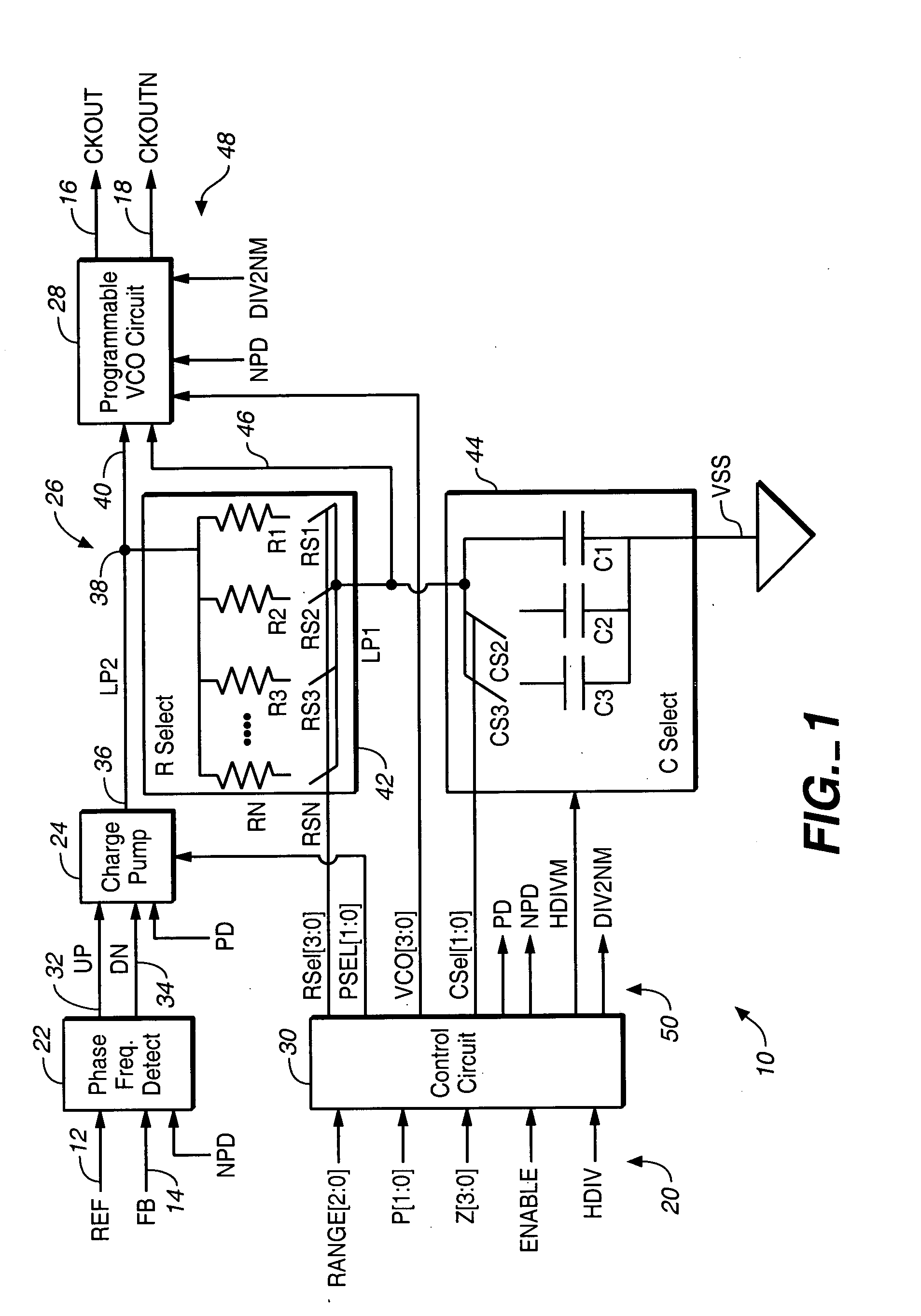
[0015]FIG. 1 is a block diagram of a phase-locked-loop (PLL) 10, which has an electrically-programmable frequency range according to one embodiment of the present invention. In this embodiment, PLL 10 is implemented as a single cell in an integrated circuit technology library, which can be selected and instantiated with other cells in an integrated circuit design for fabrication.

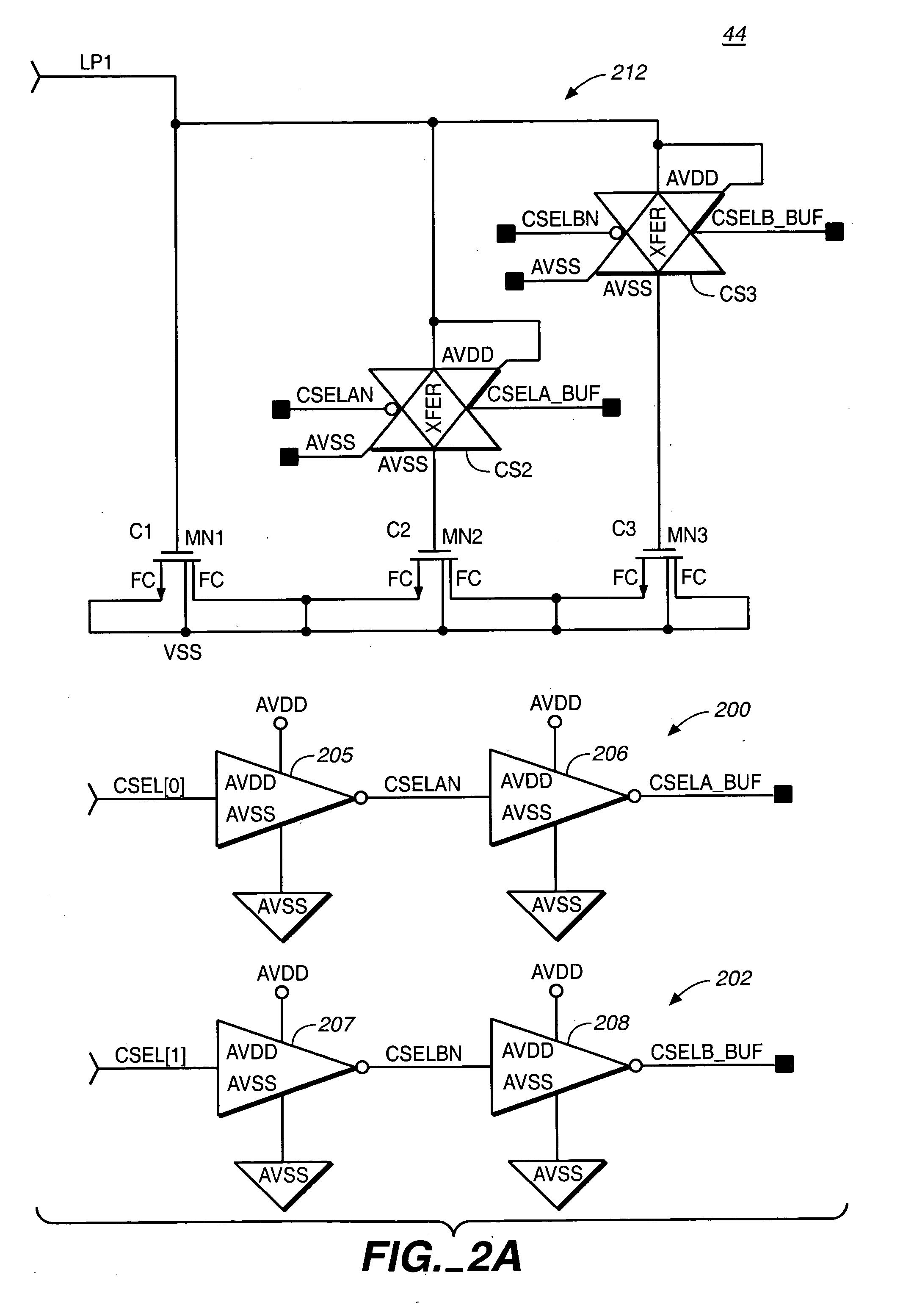
[0016] PLL10 includes a reference input 12 (labeled REF), a feedb...


PUM


Abstract

An integrated circuit is provided, which includes a phase-locked loop (PLL) that is fabricated on the integrated circuit and has a selectable loop filter capacitance and a selectable output frequency range.

Description

FIELD OF THE INVENTION [0001] The present invention relates to semiconductor integrated circuits and more particularly to implementation of phase-locked loops having different operating characteristics. BACKGROUND OF THE INVENTION [0002] Integrated circuits are generally fabricated on a thin, circular silicon wafer or substrate. Semiconductor devices and electrical interconnections that form the integrated circuit are conventionally made by building many mask layers on top of one another on the substrate. Each successive mask layer may have a pattern that is defined using a mask. A mask has a shape used for processing features in a particular process step during fabrication. The mask layers are fabricated through a sequence of pattern definition steps using the masks, which are interspersed with other process steps such as oxidation, etching, doping and material deposition. When a mask layer is defined using a mask chosen or provided by a customer, the mask layer is programmed or cu...

Claims


Application Information

Patent Timeline
IPC IPC(8): H03L7/089H03L7/093H03L7/099
CPCH03L7/0898Y10S331/02H03L7/099H03L7/093
Inventor WURZER, STEVEN G.
Owner AVAGO TECH INT SALES PTE LTD
Why Eureka
Try Eureka