Thin film transistor

a thin film transistor and gate insulating layer technology, applied in transistors, electrical devices, semiconductor devices, etc., can solve the problems of operational defects in the performance of thin film transistors, breakdown, and deterioration of achieve the effect of improving the dielectric strength of the gate insulating layer

Inactive Publication Date: 2005-06-02
SAMSUNG MOBILE DISPLAY CO LTD
View PDF12 Cites 36 Cited by
  • Summary
  • Abstract
  • Description
  • Claims
  • Application Information

AI Technical Summary

Benefits of technology

[0008] The present invention provides a thin film transistor with improved dielectric strength of a gate insulating layer.

Problems solved by technology

However, as the gate insulating layer becomes thinner, the dielectric strength of the gate insulating layer may deteriorate.
When the dielectric strength of the gate insulating layer is lower than a design value, breakdown may occur.
This may cause operational defects in the performance of the thin film transistor, and a corresponding display defect in a display device using the thin film transistor.
However, heat-oxidization in such a case requires a high temperature, thus disadvantageously requiring an expensive quartz substrate.

Method used


Image

  • Thin film transistor
  • Thin film transistor
  • Thin film transistor

Examples


example 1

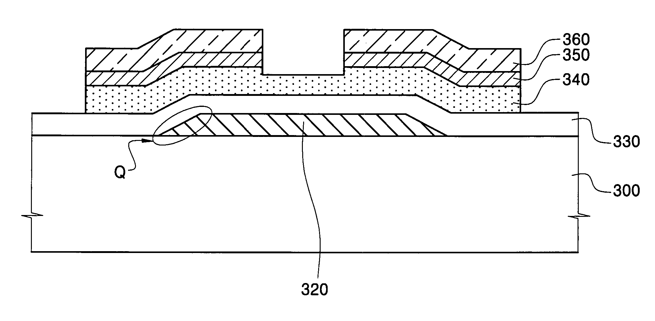
[0036] An amorphous silicon layer was formed on an insulating substrate, and was patterned to form a polysilicon layer to a thickness of 500 Å. A photoresist pattern was formed on the polysilicon layer. The polysilicon layer was etched using the photoresist pattern as a mask to form the semiconductor layer. The polysilicon was etched using SF6 / O2 gas with a ratio of 120 / 180 sccm to form a semiconductor layer. Further, a silicon oxide layer was PECVD deposited to a thickness of 1000 Å on the semiconductor layer to form a gate insulating layer. A gate electrode was formed on the gate insulating layer, thereby fabricating the example thin film transistor.

example 2

[0037] A thin film transistor, in this example, was fabricated in the same manner as the example 1 except that the polysilicon layer was etched using SF6 / O2 gas with a ratio of 100 / 200 sccm.


PUM


Abstract

A thin film transistor according to the present invention may include a gate insulating layer; and a lower pattern placed below the gate insulating layer to contact therewith and having an edge with a taper angle of at most about 80°. With this design, dielectric strength of the gate insulating layer can be enhanced. The lower pattern can be a gate electrode layer.

Description

CROSS-REFERENCE TO RELATED APPLICATION [0001] This application claims the benefit of Korean Patent Application No. 2003-85848, filed Nov. 28, 2003, the disclosure of which is incorporated herein by reference in its entirety. BACKGROUND OF THE INVENTION [0002] 1. Field of the Invention [0003] The present invention relates to a thin film transistor and, more particularly, to a thin film transistor with improved dielectric strength in a gate insulating layer. [0004] 2. Description of the Related Art [0005] Generally, a thin film transistor includes a semiconductor layer, a gate electrode, source / drain electrodes and a gate insulating layer interposed between the semiconductor layer and the gate electrode. For a circuit using the thin film transistor, there is a need to reduce the threshold voltage of the thin film transistor in order to implement high-speed operation. The threshold voltage of the thin film transistor has a close relationship with the thickness of the gate insulating la...

Claims


Application Information

Patent Timeline
Patent Type & Authority Applications(United States)
IPC IPC(8): H01L21/336H01L29/423H01L29/786
CPCH01L29/42384H01L29/66757H01L29/78678H01L29/78609H01L29/78675H01L29/66765H01L29/786
Inventor HWANG, EUI-HOONLEE, SANG-GULKIM, DEUK-JONG
Owner SAMSUNG MOBILE DISPLAY CO LTD
Why Eureka
Try Eureka