Supercharge Your Innovation With Domain-Expert AI Agents!

Thin film magnetic memory device provided with program element

a technology of magnetic memory and program element, which is applied in the direction of digital storage, semiconductor devices, instruments, etc., can solve the problems of data stored in the mtj memory cell that may be lost during heat treatment, and achieve the effect of increasing the number of manufacturing steps or manufacturing costs

Inactive Publication Date: 2005-06-02
RENESAS ELECTRONICS CORP
View PDF6 Cites 0 Cited by
  • Summary
  • Abstract
  • Description
  • Claims
  • Application Information

AI Technical Summary

Benefits of technology

This approach allows for stable and efficient programming of information across multiple manufacturing and testing stages without increasing the number of manufacturing steps or costs, enabling cumulative programming of defects detected during wafer tests, burn-in, and packaging.

Problems solved by technology

In the case of forming the program element with an excessive MTJ memory cell, however, data stored in the MTJ memory cell may be lost during heat treatment after completion of a wafer process, through burn-in and packaging steps, before shipment.

Method used


Image

  • Thin film magnetic memory device provided with program element
  • Thin film magnetic memory device provided with program element
  • Thin film magnetic memory device provided with program element

Examples


first embodiment

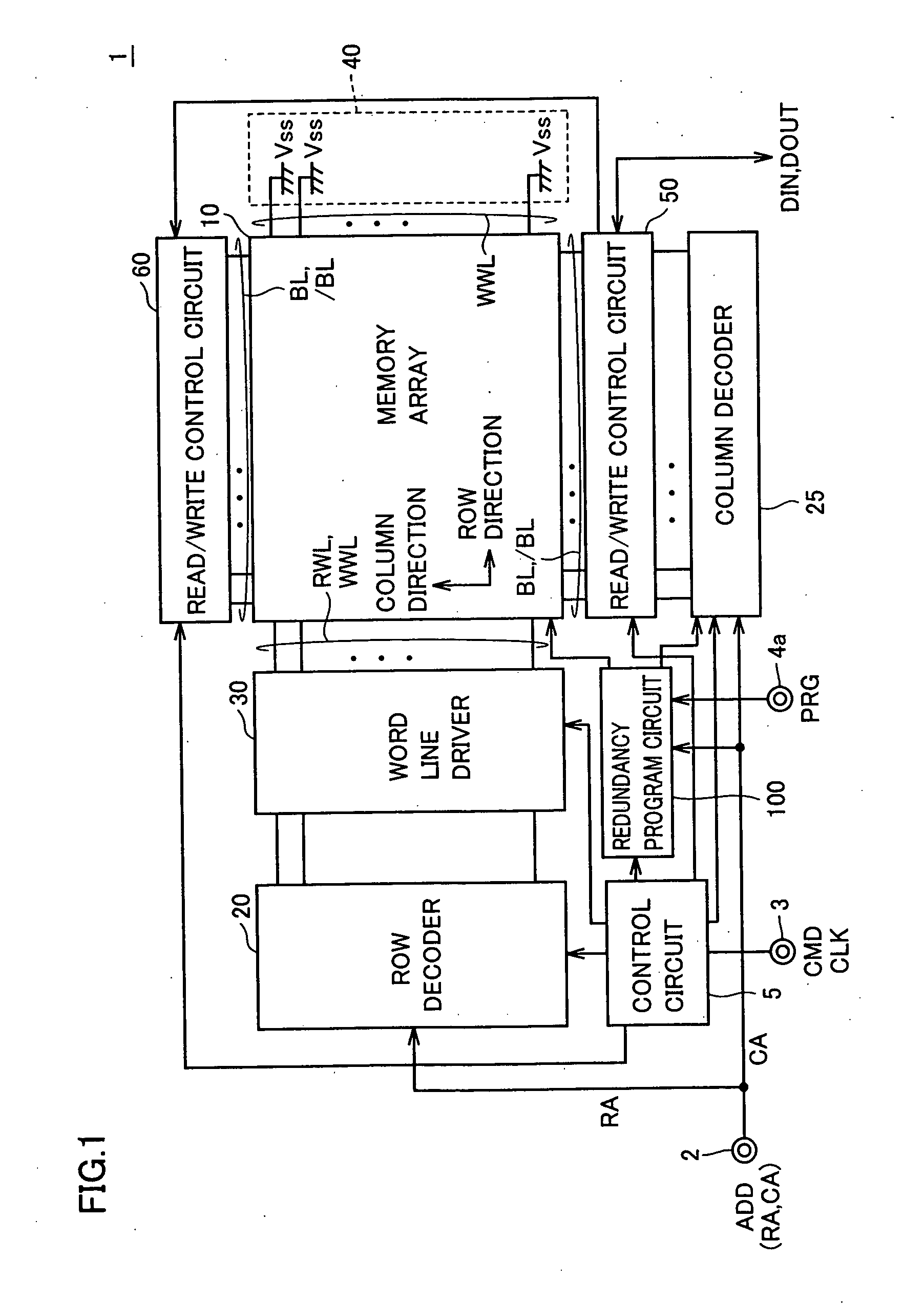
[0039] Referring to FIG. 1, the MRAM device 1 according to the first embodiment of the present invention performs random access in accordance with externally supplied control signal CMD and address signal ADD, and performs input of write data DIN and output of read data DOUT. The data read operation and the data write operation in MRAM device 1 are performed at timings in synchronization with an externally applied dock signal CLK, for example. Alternatively, the operating timings may be determined within the device, unprovided with external dock signal CLK.

[0040] MRAM device 1 includes: an address terminal 2 receiving input of address signal ADD; a control signal terminal 3 receiving input of control signal CMD and clock signal CLK; a signal terminal 4a receiving input of a control signal PRG that is activated in a program operation; a control circuit 5 for controlling the entire operations of MRAM device 1 in response to control signal CMD and clock signal CLK; and a memory array ...

second embodiment

[0150] In the second embodiment, a configuration of a program circuit employing the program element having the structure as described in the first embodiment and capable of programming information before and after a packaging step is described.

[0151]FIG. 12 is a circuit diagram showing a configuration of a redundancy control unit RPU#(i) according to the second embodiment. The MRAM device according to the second embodiment is identical to that of the first embodiment except for the configuration of each redundancy control unit. Thus, in the following, the configuration of the redundancy control unit of the second embodiment will be described in detail, while detailed description of the configurations and operations of the other portions will not be repeated.

[0152] Referring to FIG. 12, the redundancy control unit RPU#(i) of the second embodiment differs from redundancy control unit RPU(i) of the first embodiment shown in FIG. 8 in that N-MOS transistors NPT(1), / NPT(1) to NPT(h), ...

third embodiment

[0180] In the third embodiment, a configuration permitting program inputs in a plurality of steps using a program cell having the same structure as the MTJ memory cell, is described. The MRAM device of the third embodiment is identical to the MRAM device of the second embodiment except for the configurations of each program element and the program circuit. Thus, in the following, the program element and the program circuit of the third embodiment will be described in detail, and detailed description of the configurations and operations of the other portions will not be repeated.

[0181] Referring to FIG. 16, the program element according to the third embodiment has the same structure as the MTJ memory cell shown in FIG. 5. Thus, hereinafter, the program element of the third embodiment is also referred to as the program cell.

[0182] The program cell includes an access transistor ATRp formed in the same manner as access transistor ATR on a semiconductor substrate SUB, and a conductive ...


PUM


Abstract

A program element has a magnetic layer electrically connected between first and second nodes. At least a portion of the magnetic layer forms a link portion designed to be blown with external laser irradiation. The magnetic layer is provided in the same layer as and with the same structure as a tunneling magneto-resistance element in an MTJ memory cell. An electrical contact between the magnetic layer and respective one of the first and second nodes has the same structure as the electrical contact between the tunneling magneto-resistance element and an interconnection provided in the same metal interconnection layer as respective one of the first and second nodes in the MTJ memory cell.

Description

BACKGROUND OF THE INVENTION [0001] 1. Field of the Invention [0002] The present invention relates to thin film magnetic memory devices, and more particularly to a thin film magnetic memory device provided with a memory cell having a magnetic tunnel junction and a program element for storing information in a fixed manner. [0003] 2. Description of the Background Art [0004] A magnetic random access memory device (MRAM device) has attracted attention as a memory device capable of non-volatile data storage with low power consumption. The MRAM device stores data in a non-volatile manner using a plurality of thin film magnetic elements formed on a semiconductor integrated circuit, and permits random access to the respective thin film magnetic element. [0005] In particular, it has been reported that provision of memory cells (hereinafter, also referred to as “MTJ memory cells”) formed of thin film magnetic elements utilizing magnetic tunnel junctions (MTJ) significantly improves the perform...

Claims


Application Information

Patent Timeline
Patent Type & Authority Applications(United States)
IPC IPC(8): G11C11/15G11C29/04H01L21/8246H01L27/105H01L43/08
CPCG11C11/15G11C29/785G11C29/44G11C11/16
Inventor HIDAKA, HIDETO
Owner RENESAS ELECTRONICS CORP
Features
  • R&D
  • Intellectual Property
  • Life Sciences
  • Materials
  • Tech Scout
  • Unparalleled Data Quality
  • Higher Quality Content
  • 60% Fewer Hallucinations
Learn More