

Thin film magnetic memory device provided with program element
a technology of magnetic memory and program element, which is applied in the direction of digital storage, semiconductor devices, instruments, etc., can solve the problems of data stored in the mtj memory cell that may be lost during heat treatment, and achieve the effect of increasing the number of manufacturing steps or manufacturing costs
- Summary
- Abstract
- Description
- Claims
- Application Information
AI Technical Summary
Benefits of technology
Problems solved by technology
Method used
Image

Examples
first embodiment
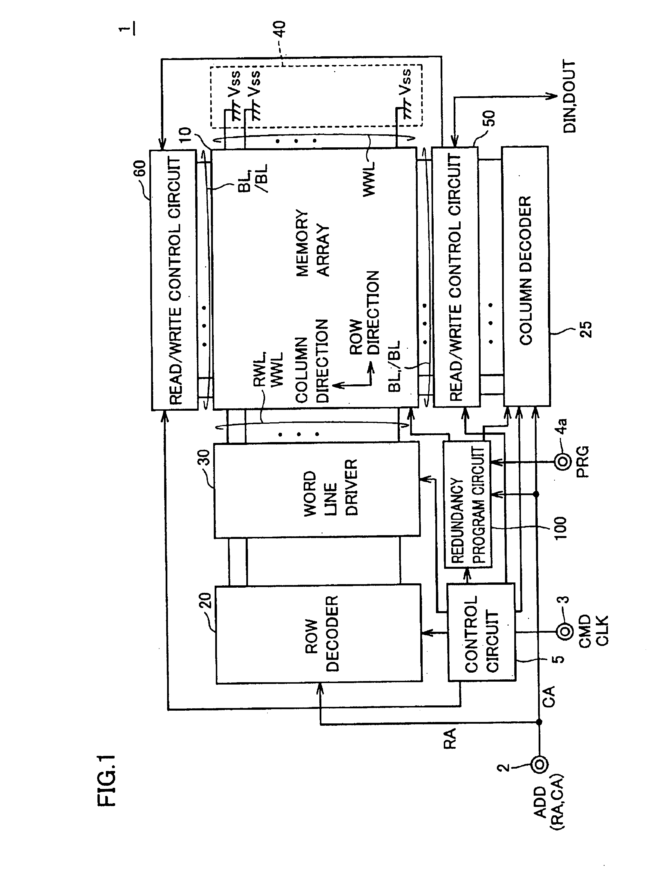
Referring to FIG. 1, the MRAM device 1 according to the first embodiment of the present invention performs random access in accordance with externally supplied control signal CMD and address signal ADD, and performs input of write data DIN and output of read data DOUT. The data read operation and the data write operation in MRAM device 1 are performed at timings in synchronization with an externally applied clock signal CLK, for example. Alternatively, the operating timings may be determined within the device, unprovided with external clock signal CLK.
MRAM device 1 includes: an address terminal 2 receiving input of address signal ADD; a control signal terminal 3 receiving input of control signal CMD and clock signal CLK; a signal terminal 4a receiving input of a control signal PRG that is activated in a program operation; a control circuit 5 for controlling the entire operations of MRAM device 1 in response to control signal CMD and clock signal CLK; and a memory array 10 having a p...
second embodiment
In the second embodiment, a configuration of a program circuit employing the program element having the structure as described in the first embodiment and capable of programming information before and after a packaging step is described.
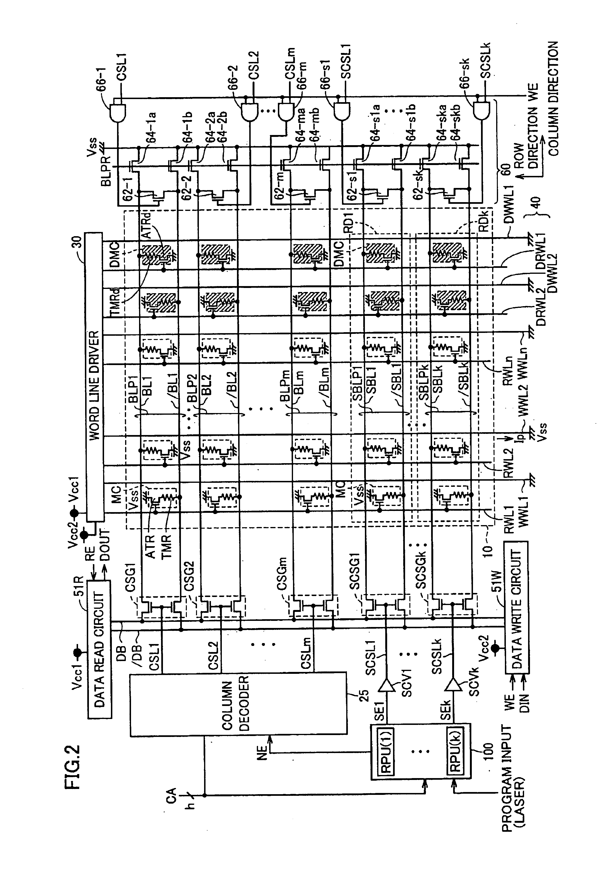
FIG. 12 is a circuit diagram showing a configuration of a redundancy control unit RPU#(i) according to the second embodiment. The MRAM device according to the second embodiment is identical to that of the first embodiment except for the configuration of each redundancy control unit. Thus, in the following, the configuration of the redundancy control unit of the second embodiment will be described in detail, while detailed description of the configurations and operations of the other portions will not be repeated.
Referring to FIG. 12, the redundancy control unit RPU#(i) of the second embodiment differs from redundancy control unit RPU(i) of the first embodiment shown in FIG. 8 in that N-MOS transistors NPT(1), / NPT(1) to NPT(h), / NPT(h) are connected ...
third embodiment
In the third embodiment, a configuration permitting program inputs in a plurality of steps using a program cell having the same structure as the MTJ memory cell, is described. The MRAM device of the third embodiment is identical to the MRAM device of the second embodiment except for the configurations of each program element and the program circuit. Thus, in the following, the program element and the program circuit of the third embodiment will be described in detail, and detailed description of the configurations and operations of the other portions will not be repeated.
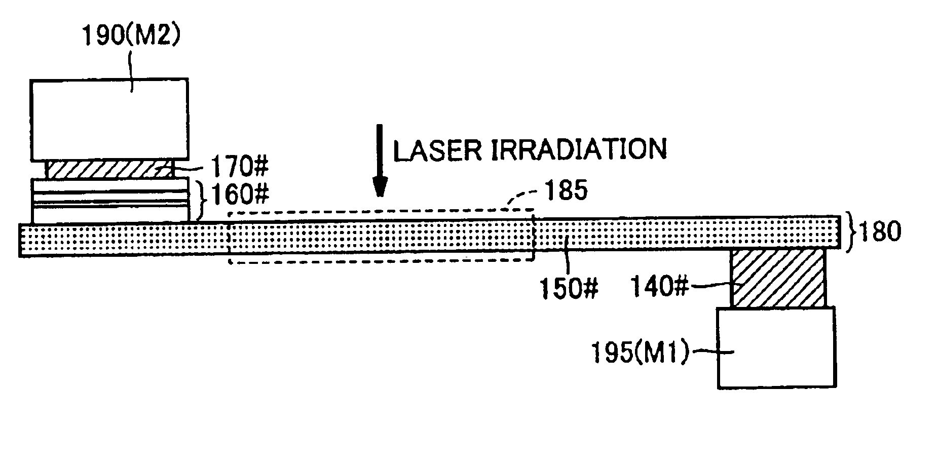
Referring to FIG. 16, the program element according to the third embodiment has the same structure as the MTJ memory cell shown in FIG. 5. Thus, hereinafter, the program element of the third embodiment is also referred to as the program cell.
The program cell includes an access transistor ATRp formed in the same manner as access transistor ATR on a semiconductor substrate SUB, and a conductive magnetic film 105# incl...
PUM
 Abstract
Description
Claims
Application Information