This helps you quickly interpret patents by identifying the three key elements:
Problems solved by technology
Method used
Benefits of technology
Benefits of technology
[0021] The method of fabricating the Gated-FET may have one or more of following advantages. A Gated-FET is constructed with Ill-V semiconductor material. A Gated-FET is constructed with poly-crystalline semiconductor thin film transistors. A Gated-FET is constructed with amorphous poly-Silicon semiconductor thin film transistors. A Gated-FET is constructed with laser re-crystallized poly-Silicon semiconductor thin film transistors. A Gated-FET is constructed on SOI material, or thinned down region of SOI material. A thinned down crystalline SOI Gated-FET has very high performance. The Gated-FET is fabricated in poly-crystalline Silicon layers with good on and off device characteristics. A circuit may be constructed with a conventional MOSFET device, and a new Gated-FET vertically integrated. A TFT module layer may be inserted to a logic process module. The TFT module layer may be inserted to SOI process module. The module insertion may be at a first contact layer. The module insertion may be at a later via layer.
[0022] Implementation of the new device may have one or more following advantages. Gated-FETs are used to build circuits and latches. Inexpensive latches are built with 3D integrated Gated-FET devices. Latches are vertically integrated to a logic process for FPGA applications. A split latch is constructed with regular MOSFET in a first layer, and vertically integrated Gated-FET in a second layer connected back to back. A s
Problems solved by technology
The reverse bias control gate junction consumes a low level of power due to carrier recombination inside the depleted region.
Due to non-overlapping gate voltages and the high voltage range thus needed, a complementary JFET process is impractical to realize.
Hence there is no low cost process that provides CJFET devices analogous to CMOS devices.
Compared to MOSFETs, JFETs also have poorer switching characteristics due to
Method used
Image
Click on the blue label to locate the original text in one second.
Reading with bidirectional positioning of images and text.
Examples
Example
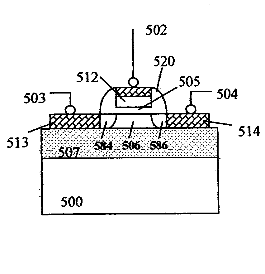
[0038] The terms wafer and substrate used in the following description include any structure having an exposed surface with which to form the Gated-FET structure of the invention. The term substrate is understood to include semiconductor wafers. The term substrate is also used to refer to semiconductor structures during processing, and may include other layers that have been fabricated thereupon. The term layer is used for processing steps used in the manufacturing process. The term layer also includes each of the masking layers of the process. Both wafer and substrate include doped and undoped semiconductors, epitaxial semiconductor layers supported by a base semiconductor or insulator, SOI material as well as other semiconductor structures well known to one skilled in the art. The term conductor is understood to include semiconductors, and the term insulator is defined to include any material that is less electrically conductive than the materials referred to as conductors. The te...
PUM
Abstract
A new Insulated-Gate Field-Effect Thin Film Transistor (Gated-FET) is disclosed. A semiconductor thin film Gated-FET device, comprising: a lightly doped resistive channel region formed on a semiconductor thin film layer, the thickness of the channel comprising the entire thin film thickness; and an insulator layer deposited on said channel surface with a gate region formed on a gate material deposited on said insulator layer, said gate region receiving a gate voltage comprised of: a first level that modulate said channel resistance to a substantially non-conductive state by fully depleting majority carriers from said thin film layer in the channel region; and a second level that modulate said channel resistance to a substantially conductive state by at least partially accumulating majority carriers near the gate surface of the thin film layer in said channel region.
Description
[0001] This application is a division of application Ser. No. 10 / 62,627 filed on Jan. 23, 2004, which is a division of application Ser. No. 10 / 413,808 filed on Apr. 14, 2003, which claims benefit from Provisional Application Ser. No. 60 / 393,763 filed on Jul. 08, 2002, Provisional Application Ser. No. 60 / 397,070 filed on Jul. 22, 2002, Provisional Application Ser. No. 60 / 400,007 filed on Aug. 01, 2002, Provisional Application Ser. No. 60 / 402,573 filed on Aug. 12, 2002, and Provisional Application Ser. No. 60 / 449,011 filed on Feb. 24, 2003, all of which list as inventor Mr. R. U. Madurawe and the contents of which are incorporated-by-reference. [0002] This application is also related to application Ser. No. 10 / 267,484, Application Ser. No. 10 / 267,483, and application Ser. No. 10 / 267,511 now U.S. Pat. No. 6,747,478, all of which were filed on Oct. 08, 2002 and list as inventor Mr. R. U. Madurawe, the contents of which are incorporated-by-reference.BACKGROUND [0003] The present inventio...
Claims
Application Information
Patent Timeline
Application Date:The date an application was filed.
Publication Date:The date a patent or application was officially published.
First Publication Date:The earliest publication date of a patent with the same application number.
Issue Date:Publication date of the patent grant document.
PCT Entry Date:The Entry date of PCT National Phase.
Estimated Expiry Date:The statutory expiry date of a patent right according to the Patent Law, and it is the longest term of protection that the patent right can achieve without the termination of the patent right due to other reasons(Term extension factor has been taken into account ).
Invalid Date:Actual expiry date is based on effective date or publication date of legal transaction data of invalid patent.

