Semiconductor device package utilizing proud interconnect material

a technology of proud interconnect and semiconductor devices, applied in the direction of manufacturing tools, welding/cutting media/materials, manufacturing tools, etc., can solve problems such as manufacturing complexity, and achieve the effect of reducing critical manufacturing tolerances and being easy to produ

Inactive Publication Date: 2005-06-09
INFINEON TECH AMERICAS CORP
View PDF5 Cites 51 Cited by
  • Summary
  • Abstract
  • Description
  • Claims
  • Application Information

AI Technical Summary

Benefits of technology

[0015] e) It will reduce critical manufacturing tolerances, and therefore makes the device easier to produce.

Problems solved by technology

Thus, to join a component and a conductive pad on a circuit board using the conventional technique described herein the stenciling of the solder on the circuit board (or the component) requires strict adherence to certain tolerances which complicates manufacturing.

Method used


Image

  • Semiconductor device package utilizing proud interconnect material
  • Semiconductor device package utilizing proud interconnect material
  • Semiconductor device package utilizing proud interconnect material

Examples


Embodiment Construction

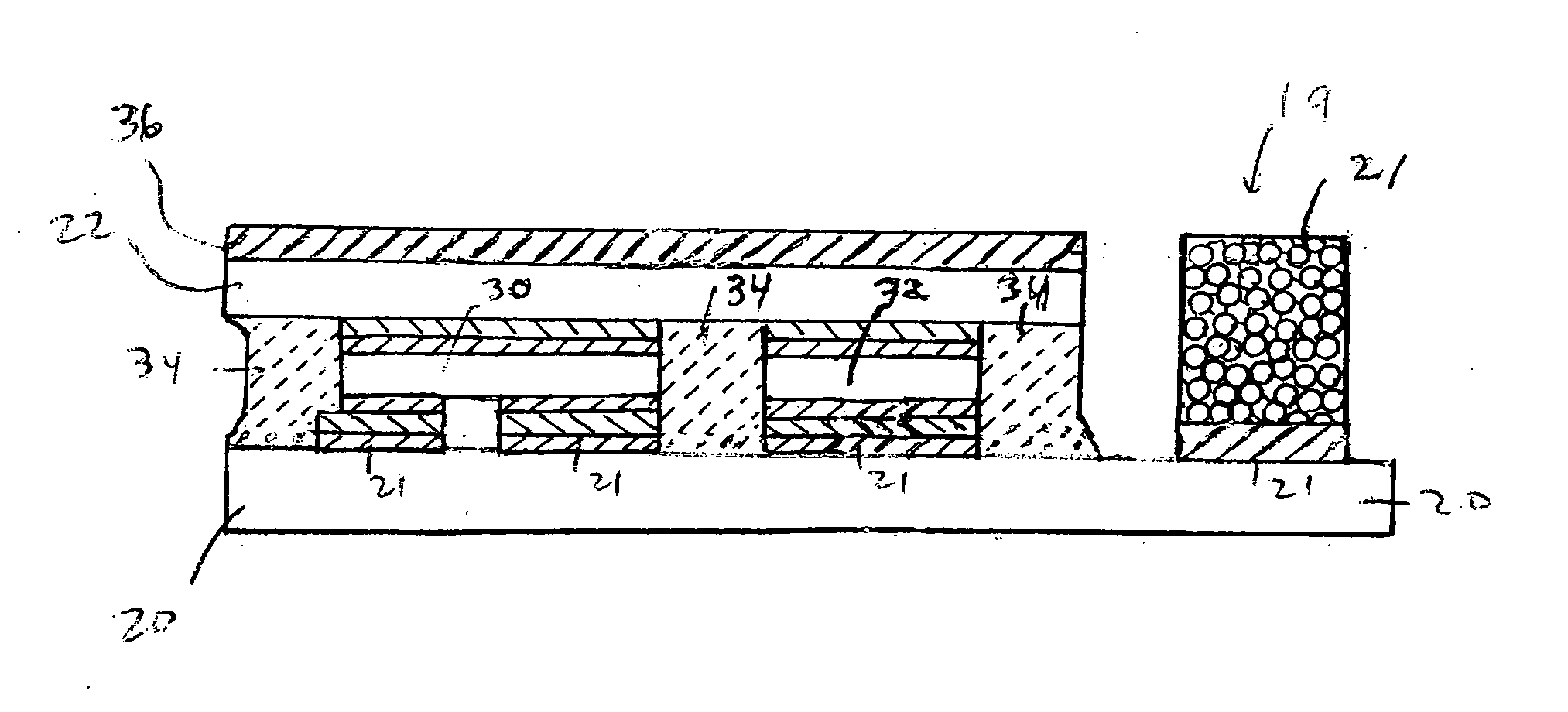
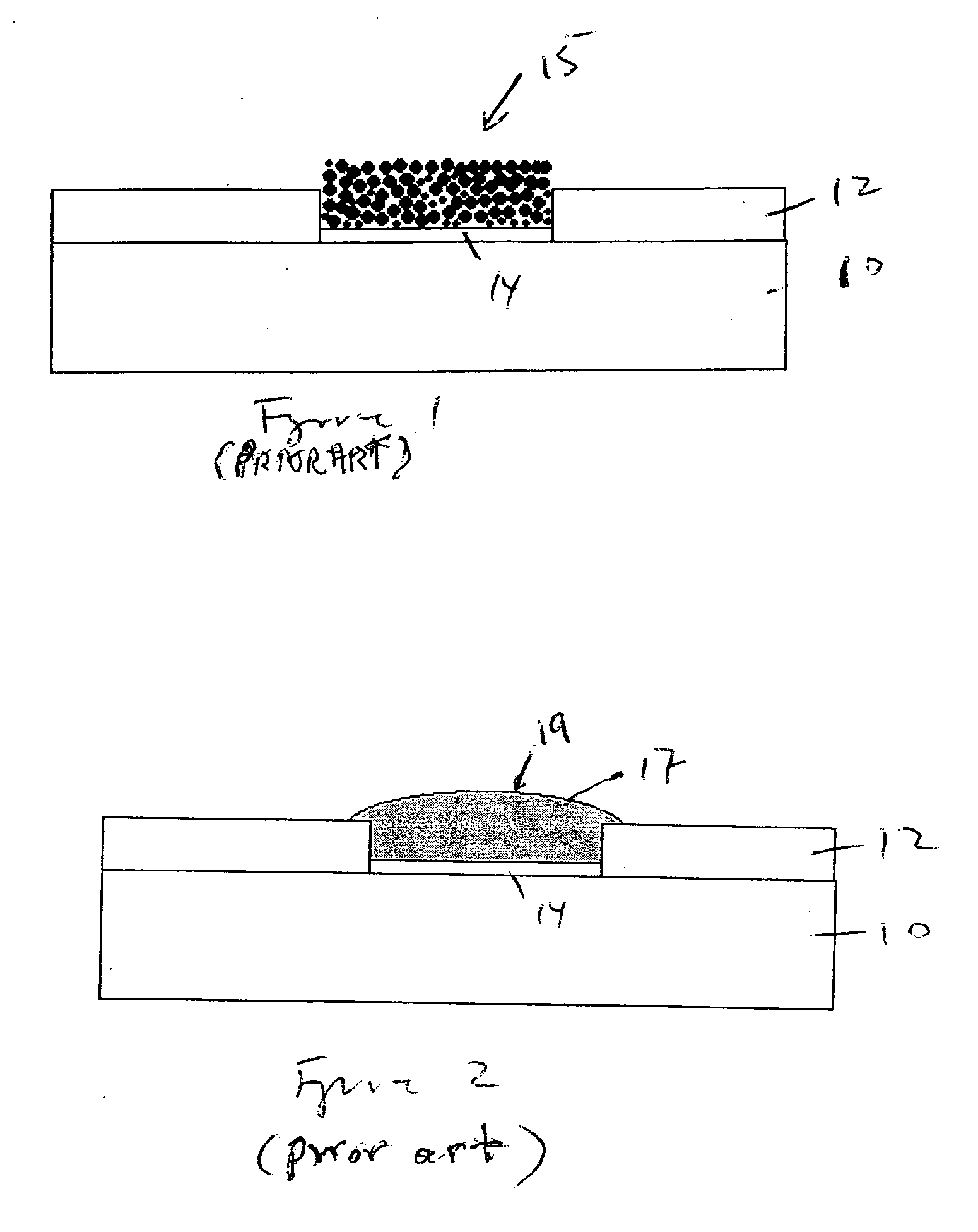
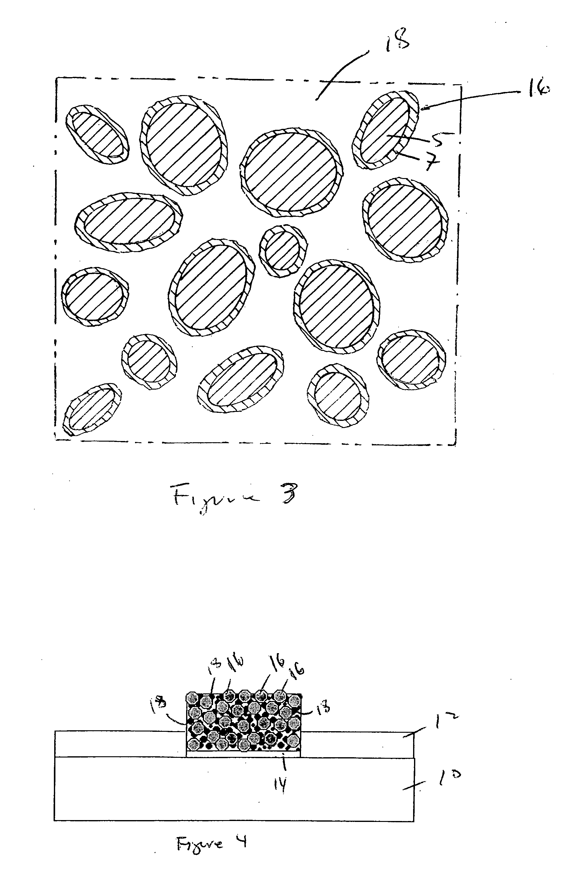
[0034] An electrically conductive paste according to the present invention includes a mixture of binder particles, and filler particles. In a preferred embodiment of the present invention, the binder particles are solder powder, and the filler particles are conductive particles dispersed throughout, or mixed in with the solder powder. The preferred embodiment further includes a solder flux material.

[0035] According to an aspect of the present invention, the proportion of the binder particles relative to the proportion of the filler particles is such that when the binder particles melt, there will be sufficient binder to fuse the filler particles, i.e., “glue” the filler particles together. However, the respective portions will be such that when binder particles are melted the shape of the paste as deposited will not change substantially. That is, the interconnect will substantially have the same shape as the paste when it is deposited.

[0036] The filler particles used in a paste ac...


PUM


Abstract

A semiconductor package which includes a conductive can, a semiconductor die received in the interior of the can and connected to an interior portion thereof at one of its sides, at least one interconnect structure formed on the other side of the semiconductor die, and a passivation layer disposed on the other side of the semiconductor die around the interconnect structure and extending at least to the can.

Description

RELATED APPLICATION [0001] The application is based on and claims priority to U.S. Provisional Application No. 60 / 514,095 filed Oct. 24, 2003, entitled Solder and Solder Process and No Flow / Reflowing Interconnects and U.S. Provisional Application No. 60 / 555,794, filed Mar. 24, 2004, entitled Semiconductor Device Package Utilizing Proud Interconnect Material.FIELD OF THE INVENTION [0002] The present invention relates to semiconductor packaging, and more particularly to an interconnect structure and a paste for forming the interconnect structure. BACKGROUND OF THE INVENTION [0003] Solder is a conventionally known material for connecting a semiconductor device to a conductive pad on a circuit board. According to a well known technique, solder bumps can be formed on a conductive pad of a circuit board, a component such as a semiconductor die can be placed thereon, and the solder is then reflown in order to connect the component to the conductive pad. Alternatively, the solder bump can b...

Claims


Application Information

Patent Timeline
Patent Type & Authority Applications(United States)
IPC IPC(8): H01LH01L21/44H01L21/60H01L23/02H01L23/48H01L23/485H01L23/52
CPCB23K35/0244B23K35/262B23K35/268B23K35/3006B23K35/302B23K35/3613H01L21/4867H01L21/56H01L23/04H01L23/13H01L23/492H01L23/49811H01L23/49827H01L23/49844H01L23/49883H01L23/5389H01L24/11H01L24/13H01L24/16H01L24/27H01L24/29H01L24/32H01L24/33H01L24/34H01L24/81H01L24/83H01L25/072H01L25/50H01L2224/13099H01L2224/13111H01L2224/16H01L2224/274H01L2224/29111H01L2224/29116H01L2224/29499H01L2224/73153H01L2224/81191H01L2224/81192H01L2224/8121H01L2224/81815H01L2224/83191H01L2224/83801H01L2224/83851H01L2924/01005H01L2924/01029H01L2924/01047H01L2924/0105H01L2924/01051H01L2924/01074H01L2924/01079H01L2924/01082H01L2924/13055H01L2924/13091H01L2924/16152H01L2224/2919H01L2924/01006H01L2924/01033H01L2924/014H01L2924/0665H01L2224/29101H01L2924/0132H01L2924/0133H01L2224/291H01L2924/157H01L2924/1579H01L2224/29455H01L2224/2929H01L2224/29311H01L2224/29347H01L2224/29355H01L2224/1181H01L2924/00013H01L2224/73253H01L24/14H01L2224/29439H01L2224/29339H01L2224/33181H01L2224/1403H01L2924/1305H01L2924/00011H01L2924/00H01L2924/01083H01L2924/00014H01L2224/29099H01L2224/29199H01L2224/29299H01L2924/12042H01L2224/40225H01L24/40H01L2224/05571H01L2224/05573H01L2224/05568H01L2224/371H01L2224/84801H01L2224/37147H01L2224/8385H01L24/37H01L2224/37599H01L24/84H01L2224/81205H01L2224/83205H01L2224/05599H01L23/4825H01L23/4827
Inventor STANDING, MARTIN
Owner INFINEON TECH AMERICAS CORP
Why Eureka
Try Eureka