
Electrode structures and method to form electrode structures that minimize electrode work function variation

a technology of electrodes and structures, applied in the direction of semiconductor/solid-state device manufacturing, basic electric elements, electric devices, etc., can solve the problems of unreliability of writing and erasing a given memory device in the array, and achieve the effect of minimizing the variation of the work function of the electrod

Inactive Publication Date: 2005-06-09
MICRON TECH INC
View PDF3 Cites 15 Cited by
  • Summary
  • Abstract
  • Description
  • Claims
  • Application Information

AI Technical Summary

Benefits of technology

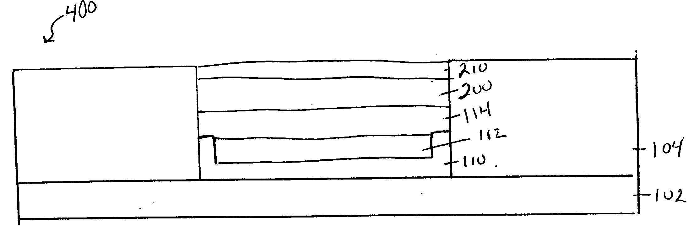
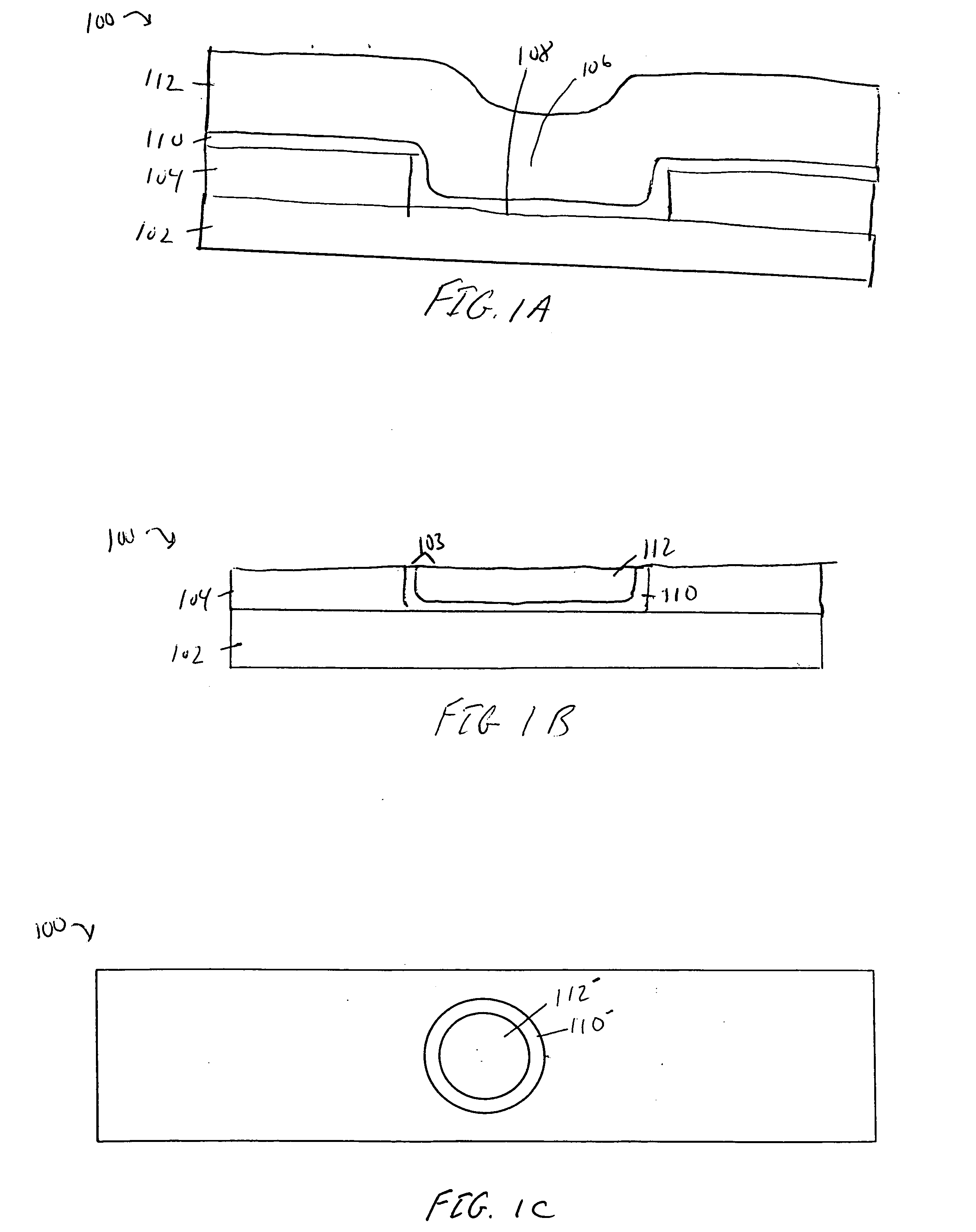
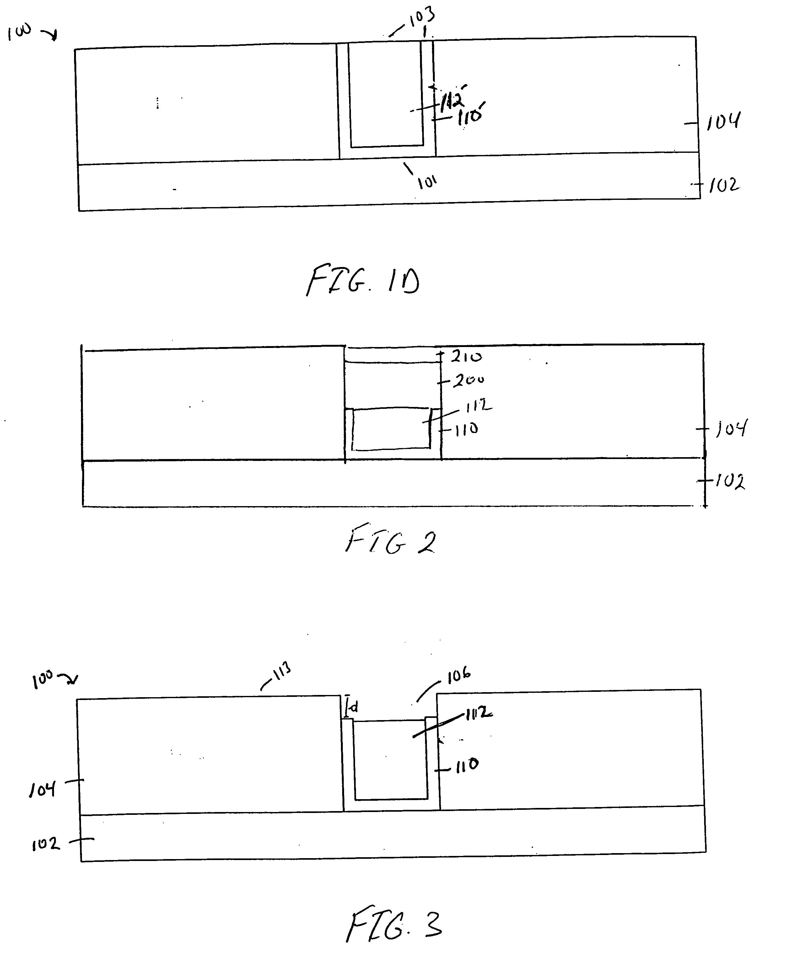
[0006] In accordance with various exemplary embodiments of the present invention, electrode structures, variable resistance memory devices, and methods of making the same, which minimize electrode work function variation, are provided. In the various embodiments, an electrode having a minimal work function variation is provided by eliminating concentric circles of electrode materials having different work functions.

Problems solved by technology

Such variation in threshold switching voltage makes writing and erasing a given memory device in the array unreliable.

Method used


Image

  • Electrode structures and method to form electrode structures that minimize electrode work function variation
  • Electrode structures and method to form electrode structures that minimize electrode work function variation
  • Electrode structures and method to form electrode structures that minimize electrode work function variation

Examples


Embodiment Construction

[0021] In the following detailed description, reference is made to various specific embodiments of the invention. These embodiments are described with sufficient detail to enable those skilled in the art to practice the invention, and it is to be understood that other embodiments may be employed, and that various structural, logical and electrical changes may be made without departing from the spirit or scope of the invention.

[0022] The present invention relates to electrode structures, variable resistance memory devices, and methods of making the same that minimize electrode workfunction variation. The workfunction of an electrode is a measure of the difficulty of escape of an electron from the electrode and is typically measured in electron volts. The lower the work function of the electrode, the greater the number of electrons that will be capable of escaping from the cathode when an electrical potential is applied thereto.

[0023] In the examples given below, the present inventi...


PUM

PropertyMeasurementUnit
recess depthaaaaaaaaaa
adhesionaaaaaaaaaa
conductiveaaaaaaaaaa

Abstract

Electrode structures, variable resistance memory devices, and methods of making the same, which minimize electrode work function variation. Methods of forming an electrode having a minimized work function variation include methods of eliminating concentric circles of material having different work functions. Exemplary electrodes include electrode structures having concentric circles of materials with different work functions, wherein this difference in workfunction has been minimized by recessing these materials within an opening in a dielectric and forming a third conductor, having a uniform work function, over said recessed materials.

Description

FIELD OF THE INVENTION [0001] The present invention relates to the field of random access memory (RAM) devices formed using a resistance variable material, and in particular to electrodes and method of forming electrodes used in resistance variable memory devices. BACKGROUND OF THE INVENTION [0002] Recently, resistance variable memory elements, which include Programmable Conductive Random Access Memory (PCRAM) elements and molecular memory elements, have been investigated for suitability as semi-volatile and non-volatile random access memory devices. A typical PCRAM device is disclosed in U.S. Pat. No. 6,348,365 assigned to Micron Technology, Inc., and hereby incorporated by reference. Typical molecular memory devices are described in U.S. Patent Application Publication No. 2002 / 0163831 to Krieger et al, which is hereby incorporated by reference. In typical PCRAM devices, conductive material, such as silver, is incorporated into a chalcogenide material, which is positioned between t...

Claims


Application Information

Patent Timeline
Patent Type & Authority Applications(United States)
IPC IPC(8): H01L21/44H01L21/768H01L45/00
CPCH01L21/76877H01L45/085H01L45/16H01L45/1253H01L45/1233H10N70/245H10N70/841H10N70/011H10N70/826
Inventor BROOKS, JOSEPH F.MOORE, JOHN T.
Owner MICRON TECH INC
Learn More