Apparatus and method for fabricating liquid crystal display

a liquid crystal display and apparatus technology, applied in the direction of instruments, coatings, chemistry apparatus and processes, etc., can solve the problems of increasing the risk of forming an lcd panel b>100/b> with a defective seal pattern b>116, increasing material expenses incurred during lcd panel fabrication, and reducing the efficiency with which lcd panels b>100/b> are fabricated, so as to reduce the time required, minimize the introduction foreign

Active Publication Date: 2005-06-16
LG DISPLAY CO LTD
View PDF43 Cites 37 Cited by
  • Summary
  • Abstract
  • Description
  • Claims
  • Application Information

AI Technical Summary

Benefits of technology

[0020] An advantage of the present invention provides an apparatus and a method for fabricating an LCD panel that can increase the reliability of a seal pattern examination process while reducing the time required to perform such an examination process.
[0021] Another advantage of the present invention provides an apparatus and a method for fabricating an LCD panel that can minimize the introduction of foreign materials onto a substrate and can increase the efficiency with which LCD panels are fabricated.
[0022] Still another advantage of the present invention provides an apparatus and a method for fabricating an LCD panel whereby subsequent processes are not performed on LCD panels having defective seal patterns, thereby minimizing the material expenses incurred during LCD panel fabrication.
[0023] Yet another advantage of the present invention provides an apparatus and a method for fabricating an LCD panel incorporating a buffer unit, thereby allowing seal patterns of consecutively-loaded substrates to be examined without stopping the LCD panel production line.
[0024] Still a further advantage of the present invention provides an apparatus and a method for fabricating an LCD panel capable of efficiently operating an LCD panel production line.
[0025] Additional features and advantages of the invention will be set forth in the description which follows, and in part will be apparent from the description, or may be learned by practice of the invention. These and other advantages of the invention will be realized and attained by the structure particularly pointed out in the written description and claims hereof as well as the appended drawings.

Problems solved by technology

Moreover, because the examination process is performed only periodically, there is an increased likelihood that seal patterns 116 with defective breaks (e.g., breaks in portions of the seal pattern 116 other than the liquid crystal injection hole), will pass through the seal pattern forming equipment undetected, increasing the risk of forming an LCD panel 100 with a defective seal pattern 116.
As a consequence, material expenses incurred during LCD panel fabrication increase.
Lastly, because an operator must stop the LCD panel production line to opens the seal pattern forming equipment to examine the seal pattern 116, and then restart the LCD panel production line to resume fabrication of the LCD panels, the related art examination process reduces the efficiency with which LCD panels 100 are fabricated.

Method used


Image

  • Apparatus and method for fabricating liquid crystal display
  • Apparatus and method for fabricating liquid crystal display
  • Apparatus and method for fabricating liquid crystal display

Examples


Embodiment Construction

[0038] Reference will now be made in detail to embodiments of the present invention, examples of which are illustrated in the accompanying drawings.

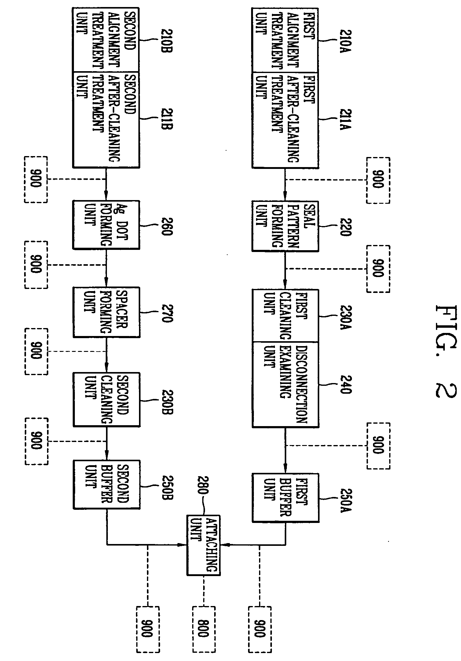
[0039]FIG. 2 illustrates an exemplary block diagram of an apparatus for fabricating an LCD panel in accordance with principles of the present invention.

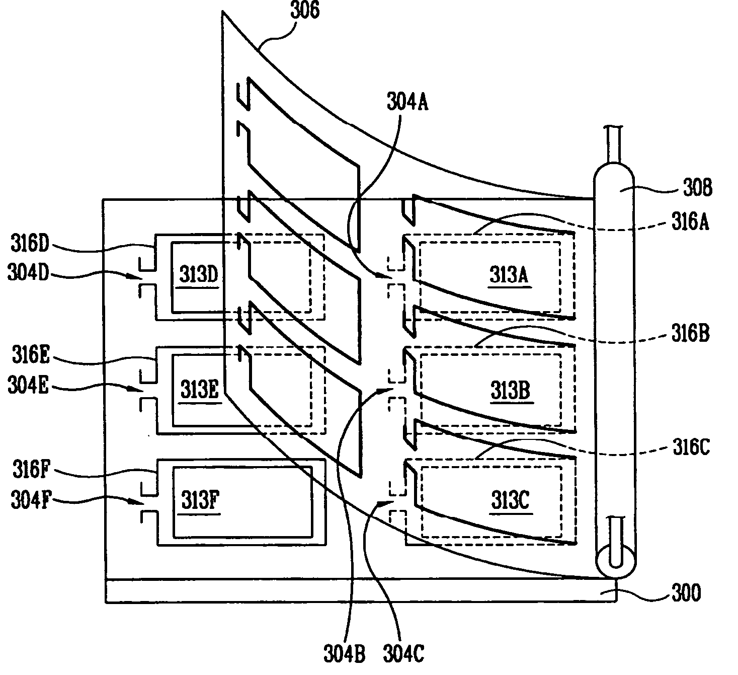
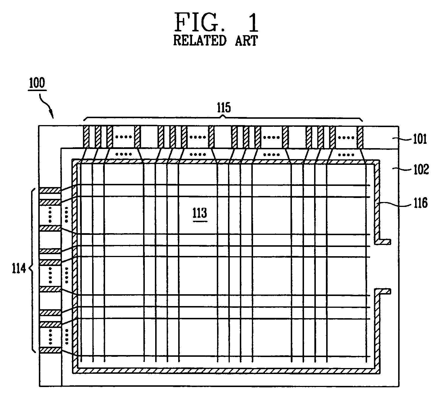
[0040] Referring to FIG. 2, the principles of the present invention provide an apparatus for fabricating an LCD panel. The apparatus may, for example, include first and second alignment treatment units 210A and 210B for forming alignment films on respective ones of the first and second base substrates; a seal pattern forming unit 220 for forming seal patterns on the alignment-treated first base substrate; a first cleaning unit 230A for cleaning the first base substrate, on which the seal patterns have been formed; a disconnection examining unit 240 coupled to the first cleaning unit 230A for examining the first base substrate to determine the existence of defective breaks in the seal pa...


PUM

PropertyMeasurementUnit
shapeaaaaaaaaaa
widthaaaaaaaaaa
vacuumaaaaaaaaaa

Abstract

An apparatus for fabricating an LCD panel includes first and second alignment treatment units for performing alignment treatments on first and second base substrates, a seal pattern forming unit for forming at least one seal pattern on the alignment-treated first base substrate, a cleaning unit for cleaning the first base substrate on which the at least one seal pattern has been formed, a disconnection examining unit operatively coupled to the cleaning unit for examining the at least one seal pattern to determined the presence of defective breaks in the at least one seal pattern, first and second buffer units for temporarily holding the first and second base substrates, respectively, and an attaching unit for loading the temporarily held first and second base substrates and for attaching the loaded first and second base substrates.

Description

[0001] This application claims the benefit of Korean Patent Application No. 90982 / 2003, filed on Dec. 13, 2003, which is hereby incorporated by reference for all purposes as if fully set forth herein. BACKGROUND OF THE INVENTION [0002] 1. Field of the Invention [0003] The present invention relates to an apparatus and a method for fabricating liquid crystal display (LCD) panels. More particularly, the present invention relates to an apparatus and a method for efficiently examining seal patterns used in attaching substrate together. [0004] 2. Discussion of the Related Art [0005] Generally, LCD devices display images by applying data signals to an array of pixels to thereby control light transmittance characteristics of the pixels, wherein the data signals are derived from external image information. A typical LCD device includes a unit LCD panel having a plurality of pixels arranged in a matrix pattern, and gate and data driving units for driving the pixels. [0006] The LCD panel typic...

Claims


Application Information

Patent Timeline
Patent Type & Authority Applications(United States)
IPC IPC(8): B05C11/00B44C1/165G02F1/1333G02F1/13G02F1/1339G02F1/1341
CPCG02F1/1339G02F2001/133354G02F1/1341G02F1/133354G02F1/13
Inventor KIM, KWANG-JIN
Owner LG DISPLAY CO LTD
Why Eureka
Try Eureka