Strained finFETs and method of manufacture

a technology of finfets and finfets, which is applied in the direction of semiconductor devices, electrical apparatus, transistors, etc., can solve the problems of difficult process implementation, difficult use of ge %, and general disadvantages of nfet performance over pfet performan

Active Publication Date: 2005-06-16
GLOBALFOUNDRIES US INC
View PDF98 Cites 92 Cited by
  • Summary
  • Abstract
  • Description
  • Claims
  • Application Information

AI Technical Summary

Benefits of technology

[0013] In another aspect, a method of manufacturing a structure includes forming shallow trench isolation (STI) in a substrate with a first material and forming a first island associated with a pFET region and a second material forming a second island associated with an nFET region. A hard mask under tension is formed over the pFET region and the NFET region, which is used to form pFET fin and an NFET fin with a capping layer of the hard mask in the pFET region and the NFET region, respectively. Epitaxial silicon sidewalls are grown on the pFET fin and the NFET fin, where the capping layer prevents buckling of the nFET fin during the formation of the sidewall.
[0014] In another aspect of the invention, a semiconductor structure includes a substrate and a relaxed shallow trench isolation (STI) in the substrate. A first finFET comprised of a first material having a first lattice constant and a cap of highly tensile material is provided. A second finFET comprised of a second material having a second lattice constant and a cap of highly tensile material is also provided. A Si epitaxially grown sidewall is provided on the first finFET and the second finFET. The cap of highly tensile material on the second finFET prevents lateral buckling of the second finFET when the Si epitaxial sidewall is grown.

Problems solved by technology

However, the same stress component, either tensile stress or compressive stress, discriminatively affects the characteristics of an n-type device and a p-type device.
That is, because the type of stress which is beneficial for the performance of an nFET is generally disadvantageous for the performance of the pFET.
Unfortunately, the tensilely strained Si on relaxed SiGe can apply only biaxial tensile stress on the Si cap as used in stack form.
This level of Ge % is difficult to implement into processes and is not very manufacturable with major issues including surface roughness, process complexity, defect and yield control, to name but a few.
Given that a high Ge % is hard to use for the pFET (since it would be detrimental because of the relatively low levels of tension), other methods must be devised to improve the device performance.
However, the Si:C part of the structure is not relaxed.
The problem with this approach is that the mobility is not enhanced, but retarded, depending on the C content, from scattering.
While these methods do provide structures that have tensile stresses being applied to the nFET device and compressive stresses being applied along the longitudinal direction of the pFET device, they may require additional materials and / or more complex processing, and thus, resulting in higher cost.

Method used


Image

  • Strained finFETs and method of manufacture
  • Strained finFETs and method of manufacture
  • Strained finFETs and method of manufacture

Examples


Embodiment Construction

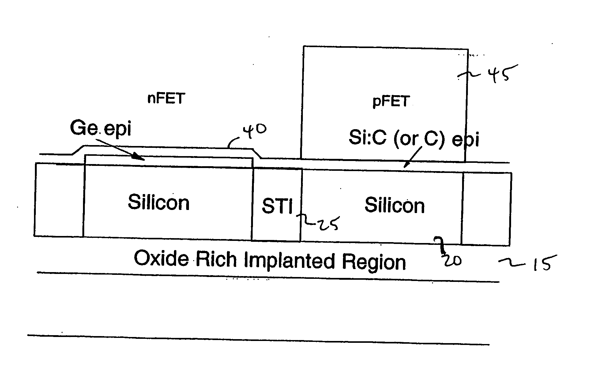
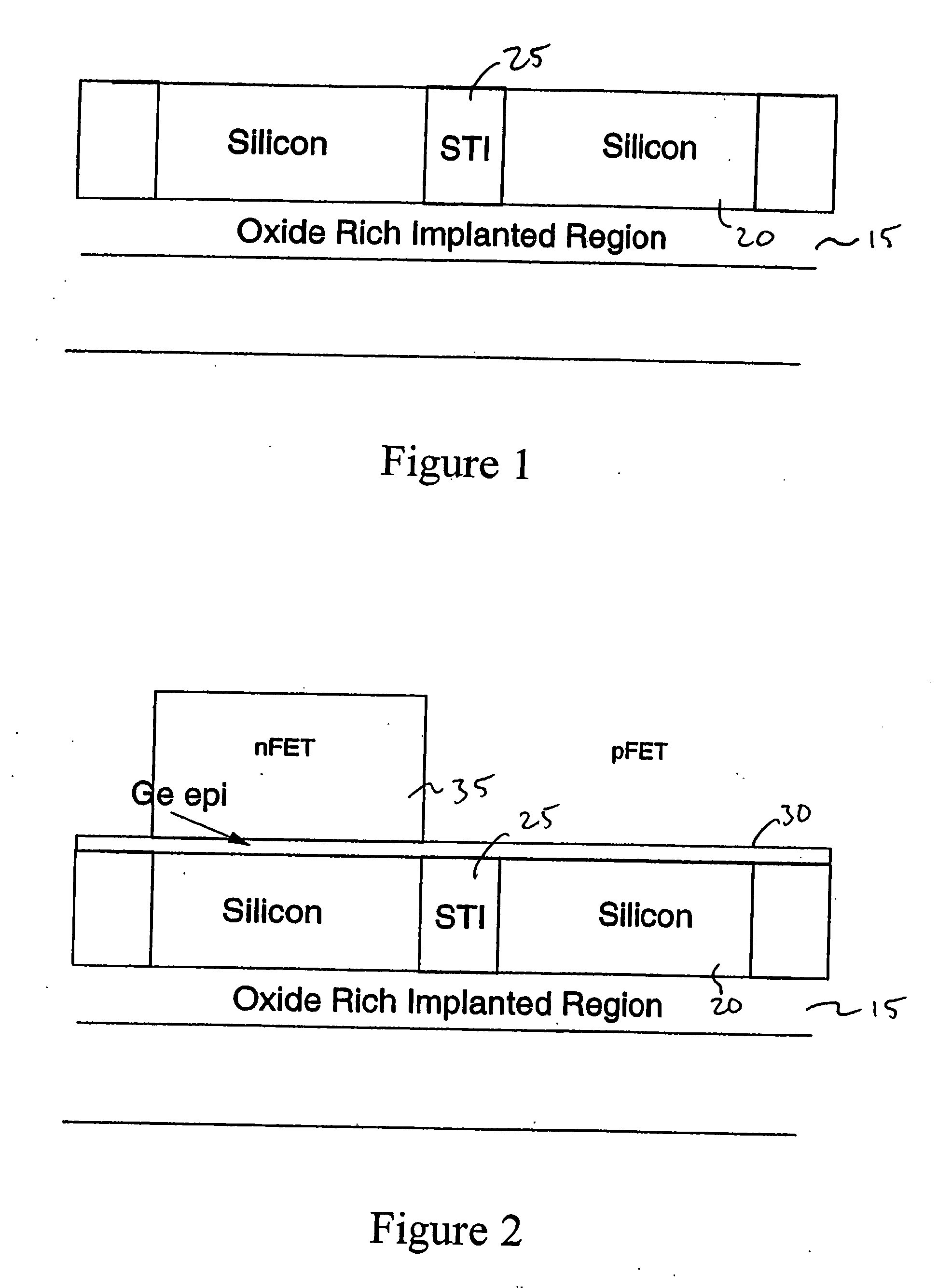
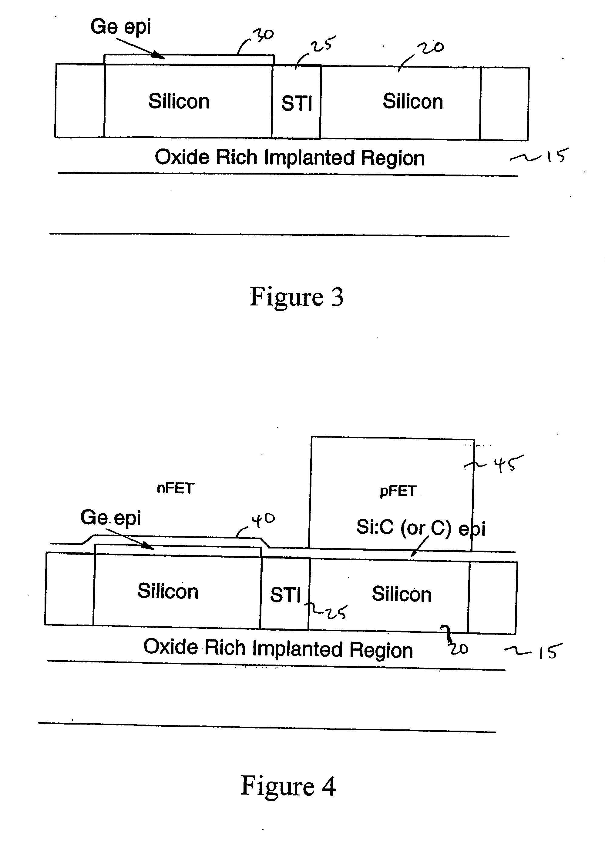
[0018] This invention is directed to a semiconductor device and method of manufacture which provides desired stresses associated with the nFET and the pFET of CMOS devices for improved device performance. In one approach, SiGe and Si:C islands are obtained in the respective nFET and pFET channels prior to the formation of finFETs. Thereafter a tensile film is formed on the islands. This tensile film, e.g., hard mask, provides a significant amount of lateral stiffness and holds the Si:C fin in place. That is, the tensile hard mask prevents the fin, which is under a highly compressive stress, from buckling, laterally, due in part to asymmetries in the fin expected to form during processing. An epitaxial Si layer is then formed on both relaxed NFET and pFET fins to provide the desired stress conditions of the NFET and the pFET.

[0019] A finFET is a double-gate structure, where the silicon body has been turned on its side to form a “fin” of silicon standing perpendicular to the wafer pl...


PUM


Abstract

A semiconductor structure and method of manufacturing is provided. The method of manufacturing includes forming shallow trench isolation (STI) in a substrate and providing a first material and a second material on the substrate. The first material and the second material form a first island and second island at an pFET region and a nFET region, respectively. A tensile hard mask is formed on the first and the second island layer prior to forming finFETs. An Si epitaxial layer is grown on the sidewalls of the finFETs with the hard mask, now a capping layer which is under tension, preventing lateral buckling of the NFET fin.

Description

BACKGROUND OF THE INVENTION [0001] 1. Field of the Invention [0002] The invention generally relates to a semiconductor device and method of manufacture and, more particularly, to the fabrication of finFETs of a semiconductor device with tensile and compressive stresses. [0003] 2. Background Description [0004] Mechanical stresses within a semiconductor device substrate can modulate device performance. That is, stresses within a semiconductor device are known to enhance semiconductor device characteristics. Thus, to improve the characteristics of a semiconductor device, tensile and / or compressive stresses are created in the channel of the n-type devices (e.g., nFETs) and / or p-type devices (e.g., pFETs). However, the same stress component, either tensile stress or compressive stress, discriminatively affects the characteristics of an n-type device and a p-type device. [0005] In order to maximize the performance of both nFETs and pFETs within integrated circuit (IC) chips, the stress co...

Claims


Application Information

Patent Timeline
Patent Type & Authority Applications(United States)
IPC IPC(8): H01L21/76H01L21/20H01L21/336H01L21/762H01L21/8238H01L21/84H01L27/08H01L27/092H01L27/12H01L29/786
CPCH01L21/823807H01L21/823821H01L21/845H01L29/78684H01L29/66795H01L29/7842H01L29/785H01L27/1211
Inventor CHIDAMBARRAO, DURESETIDOKUMACI, OMER H.GLUSCHENKOV, OLEG G.
Owner GLOBALFOUNDRIES US INC
Why Eureka
Try Eureka