Interconnecting substrate for carrying semiconductor device, method of producing thereof and package of semiconductor device

a technology for interconnecting substrates and semiconductor devices, which is applied in the manufacture of printed circuits, solid-state devices, basic electric elements, etc., can solve the problems of reducing the density of the arrangement, and reducing the accuracy of the step of exposure. , to achieve the effect of high performance capability, excellent mounting reliability and high density arrangemen

Inactive Publication Date: 2005-06-16
NEC CORP
View PDF19 Cites 42 Cited by
  • Summary
  • Abstract
  • Description
  • Claims
  • Application Information

AI Technical Summary

Benefits of technology

[0013] In light of the above problems, an object of the present invention is to provide an interconnecting substrate for carrying a semiconductor device, wherein, to match with the increase in number of terminals and the narrowing of their pitches in the semiconductor device, a higher density in arrangement and minuter interconnections are achieved, and besides, to match with a more compact and more densely spaced system, the narrowing of the pitches for the external electrodes is achieved, and, in addition, the excellent mounting reliability is attained, and a method of producing thereof as well as a package of a semiconductor device.
[0076] The present invention can achieve a higher density in arrangement and minuter interconnections in the interconnecting substrate to match with the increase in number of terminals and the narrowing of their pitches in the semiconductor device, and besides can achieve the narrowing of the pitches for the external electrodes in the interconnecting substrate to match with a more compact and more densely spaced system. Further, the present invention can provide the interconnecting substrate with excellent mounting reliability and can achieve the package of a semiconductor device with high performance capability and excellent reliability.

Problems solved by technology

However, because the glass epoxy print substrate whose heat resistance is considerably low is utilized as the base core substrate in this build-up multi-layered substrate, there arises a problem that the heat treatments performed in fabrication of the build-up multi-layered substrate may bring the glass epoxy print substrate to a poor condition, creating defects such as the shrinkage, the warp and the swell.
These defects markedly lower the accuracy in the step of exposure so that it is difficult to form a densely spaced minute interconnection pattern on the glass epoxy print substrate.
Further, when the semiconductor device is loaded on such a build-up multi-layered substrate by the flip chip method, heat treatments carried out at the time of chip loading and solder reflow are liable to cause the faulty connection and the distortion, and, therefore, liable to lower the long-term reliability for the connection.
Nevertheless, in the interconnecting substrates for packaging shown in FIG. 18, since the external electrode terminals 108 thereof are formed by etching the metal board 101, the limitation of control over the amount of side etching at the time of etching makes it extremely difficult to form the external electrode terminals 108 with narrow pitches.
Moreover, when this interconnecting substrate for packaging is mounted on an external board or apparatus, the stress is structurally centered on the interface between the external electrode terminal 108 and the insulating layer 102, which tends to give rise to opening defects so that the satisfactory mounting reliability cannot be obtained.

Method used


Image

  • Interconnecting substrate for carrying semiconductor device, method of producing thereof and package of semiconductor device
  • Interconnecting substrate for carrying semiconductor device, method of producing thereof and package of semiconductor device
  • Interconnecting substrate for carrying semiconductor device, method of producing thereof and package of semiconductor device

Examples


Embodiment Construction

[0095] The preferred embodiments of an interconnecting substrate for carrying a semiconductor device (referred to, appropriately, as an “interconnecting substrate”, hereinafter) and a package of a semiconductor device as well as producing methods of these according to the present invention are each described in detail below.

[Interconnecting Substrate]

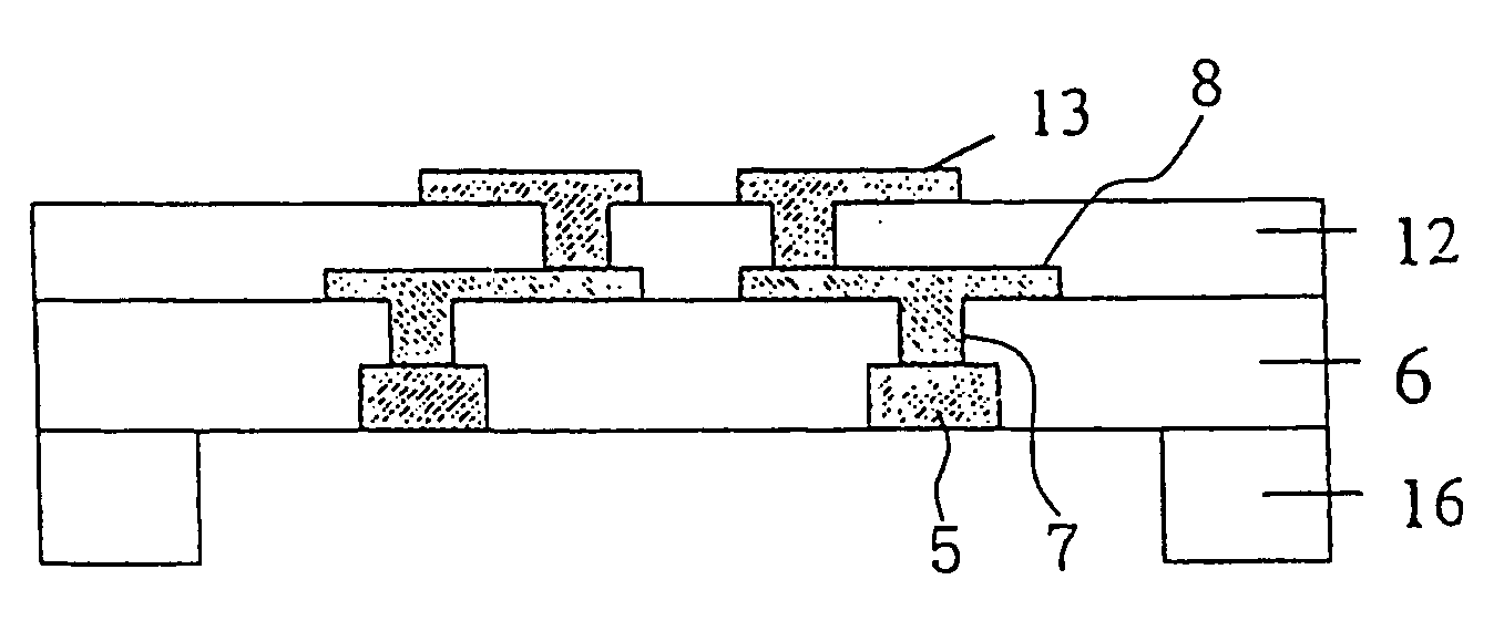
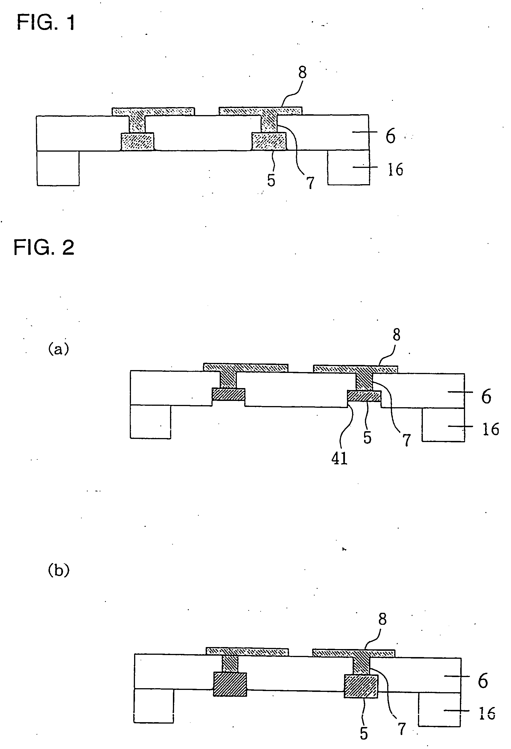
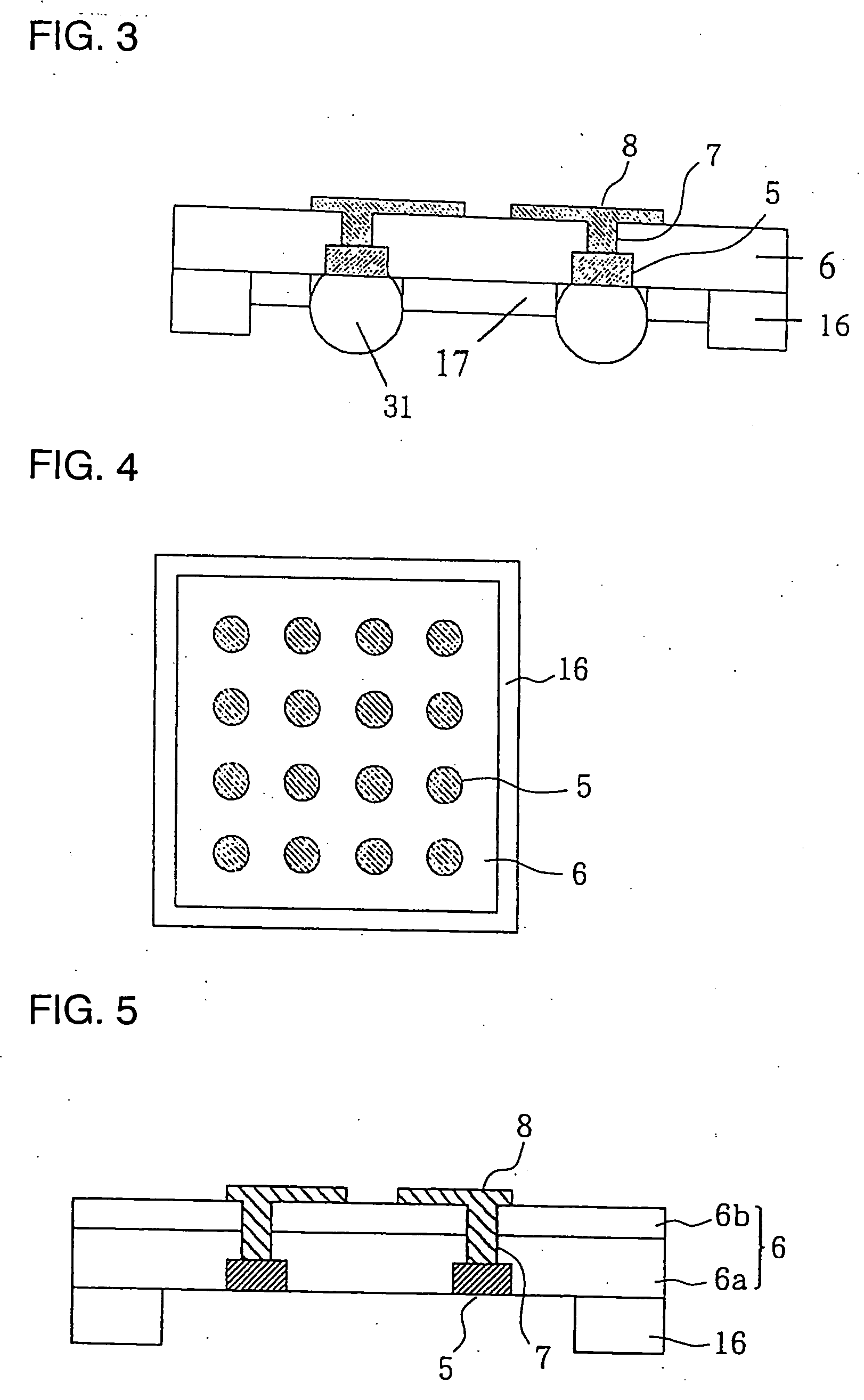
[0096]FIG. 1 is a schematic cross-sectional view showing one embodiment of an interconnecting substrate according to the present invention.

[0097] An interconnecting substrate of the present embodiment has an insulating layer 6, an interconnection 8 laid on the obverse surface of this insulating layer 6, electrodes 5 set on the reverse surface side of this insulating layer 6, via conductors 7 each of which is disposed on the obverse surface of one of these electrodes 5 and set within the insulating layer 6 so as to connect this electrode 5 with the interconnection 8, and a supporting structure 16 set on the reverse surface of the insu...


PUM


Abstract

An interconnecting substrate for carrying a semiconductor device, comprising: an insulating layer; an interconnection set on an obverse surface of the insulating layer; an electrode which is set on a reverse surface side of the insulating layer and formed in such a way that, at least, a lateral face of an obverse end of the electrode is all round brought into contact with the insulating layer, while, at least, a reverse surface of the electrode is not in contact with said insulating layer; a via conductor which is disposed on an obverse surface of the electrode and formed in the insulating layer so as to connect this electrode with the interconnection; and a supporting structure on the surface of the insulating layer.

Description

CROSS REFERENCE TO RELATED APPLICATIONS [0001] This application is a division of co-pending application Ser. No. 10 / 097,843, filed on Mar. 15, 2002, the entire contents of which are hereby incorporated by referenceTECHNICAL FIELD [0002] The present invention relates to an interconnecting substrate which is capable to carry a semiconductor device of all sorts with a high density and fittingly used to produce a high-speed, high-density module or system, and a method of producing thereof as well as a package of a semiconductor device in which the interconnecting substrate carries a semiconductor device thereon. BACKGROUND ART [0003] In recent years, accompanying the increase in the number of terminals and the narrowing of their pitches in the semiconductor device which result from advancements in the speed of operations, the capability of multi functions and the degree of integration thereof, there have been, more than ever, growing demands that the interconnecting substrate for packag...

Claims


Application Information

Patent Timeline
Patent Type & Authority Applications(United States)
IPC IPC(8): H01L21/48H01L23/498H05K1/11H05K3/20H05K3/46
CPCH01L21/4857H01L23/49822H01L23/49838H01L2221/68345H01L2224/16H01L2924/01019H01L2924/01079H05K1/112H05K3/20H05K3/4644H01L2924/01078H01L2224/05571H01L2224/05573
Inventor SHIMOTO, TADANORIKIKUCHI, KATSUMIMATSUI, KOJIBABA, KAZUHIRO
Owner NEC CORP
Why Eureka
Try Eureka