III-nitride quantum-well field effect transistors

a field effect transistor and nitride technology, applied in the field of semiconductor devices, can solve the problems of increasing the cost of semiconductor/solid-state devices, increasing the cost of semiconductor devices,

Inactive Publication Date: 2005-06-23
III N TECH +1
View PDF20 Cites 161 Cited by
  • Summary
  • Abstract
  • Description
  • Claims
  • Application Information

AI Technical Summary

Benefits of technology

[0010] The present invention provides an improved III-nitride quantum-well based field effect transistor (QW-FET) structure/device. The substrate may be Sapphire, Silicon, Silicon Carbide, or other appropriate materials. On the top of this substrate, a highly resistive thick epilayer such as Aluminum Nitride (AlN), Aluminum Gallium Nitride (AlGaN), Indium Aluminum Gallium Nitride (InAlGaN), or Aluminum Boron Nitride (AlBN), for example, is first deposited on a low temperature grown buffer layer as the epitaxial template for the subsequent layers. The low temperature buffer layer may include AIN, AlGaN, InAlGaN, AlBN,

Problems solved by technology

However, the military and modern microelectronic industries are constantly faced with demands for higher device performance.
Power amplifiers are the major factor in performance and cost for next-generation base stations.
In amplifying high-frequency RF signals, most of the power consumed is lost to heat.
This heat results in reduced reliability of these devices and systems and higher air-conditioning costs, contributing to substantially larger and more expensive base stations.
Although AlGaN/GaN HFETs have reached a high performance level, they still suffer from many problems, such as drain current collapse phenomenon.
Many of the problems are caused by parasitic conduction in the semi-insulating GaN epilayer, the s

Method used


Image

  • III-nitride quantum-well field effect transistors
  • III-nitride quantum-well field effect transistors
  • III-nitride quantum-well field effect transistors

Examples


Embodiment Construction

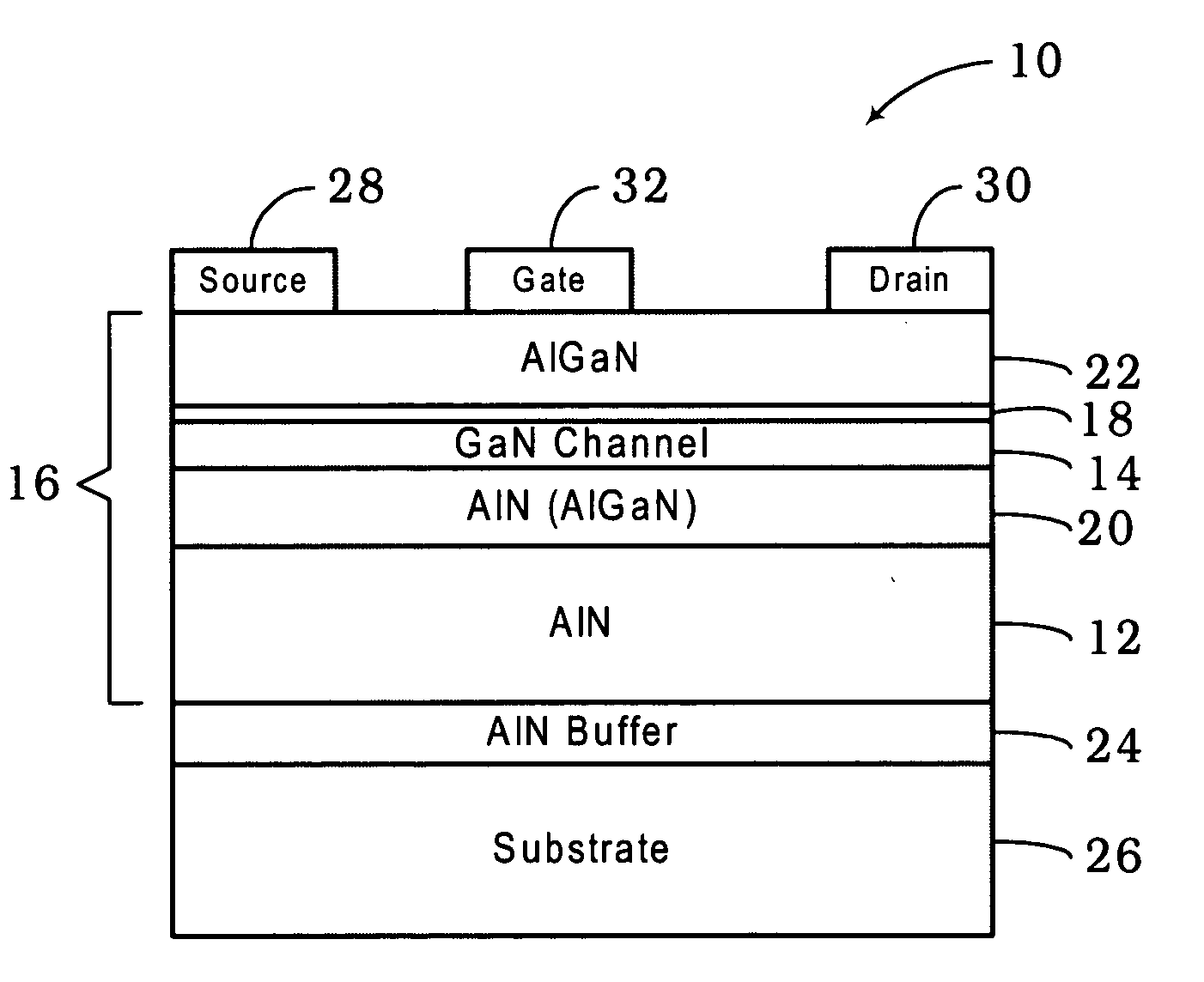
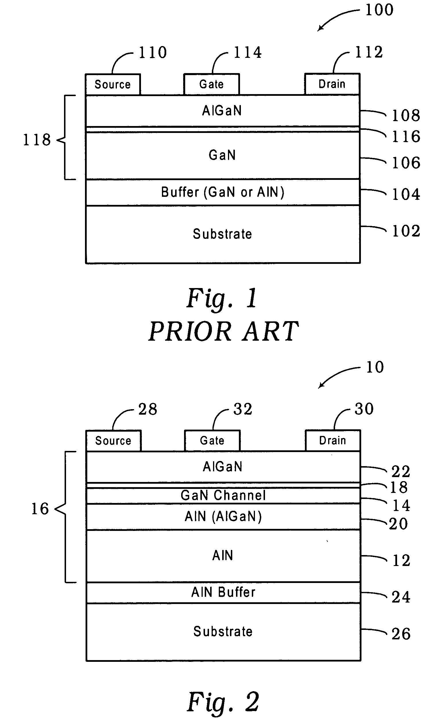
[0020] Comparing the conventional AlGaN / GaN HFET structure of the prior art illustrated in FIG. 1 with the present invention illustrated in FIG. 2, the novel QW-FET structure of this invention generally identified by reference numeral 10 incorporates several distinctive schemes. The first three include: (1) replacing the “semi-insulating” GaN epilayer 106 with a highly resistive epilayer 12, (2) employing only a thin channel layer 14 (a few tens of nanometers to a few hundreds of nanometers) instead of a thick GaN epilayer 106 (a few microns) as the channel layer, and consequently (3) substituting the conventional AlGaN / GaN single heterostructure 118 with the AlGaN / GaN / AIN(AlGaN) quantum-well structure 16. By doing so, the parasitic conduction in the thick GaN epilayer 106 and leakage current of the prior art will be completely eliminated and the drain current collapse will be reduced, and hence the amplification characteristics will be improved. Moreover, the reduction of the chann...


PUM


Abstract

A transistor with improved device characteristics includes a substrate, a first buffer layer deposited on the substrate, a highly resistive epilayer deposited on the buffer layer, a second epilayer deposited on the highly resistive epilayer, a channel layer deposited on the second epilayer, an AlGaN alloy epilayer deposited on the channel layer, and source, gate, and drain connections deposited on the AlGaN alloy epilayer. The highly resistive epilayer may include AlGaN, InAlGaN, AlBN, or AlN compositions. The channel layer may include InGaN, graded InGaN, multilayers of InGaN and GaN, or GaN.

Description

BACKGROUND OF THE INVENTION [0001] 1. Field of the Invention [0002] The present invention relates to a semiconductor device having improved device characteristics and, in particular, to a field effect transistor constructed of the AlGaN / GaN / AlN(AlGaN) quantum-well heterostructure with improved (i) amplification characteristics, (ii) power and frequency performances, and (iii) reliability and stability. [0003] 2. Description of the Prior Art [0004] Modern microelectronic devices based on semiconductor heterojunction field-effect transistors (HFETs), also called high electron mobility transistors (HEMTs) or modulation doped field effect transistor (MODFET), have a wide range of applications, including communications such as radar links, direct broadcast satellite television, cellular telephone, cable television converters, and data processing applications. These III-V compound semiconductor HFET, HEMT or MODFET devices use the high mobility property of the two-dimensional (2-D) electr...

Claims


Application Information

Patent Timeline
IPC IPC(8): H01L31/072
CPCH01L29/2003H01L29/7783H01L29/66462
Inventor FAN, ZHAOYANGLI, JINGJIANG, HONGXINGLIN, JINGYU
Owner III N TECH
Why Eureka
Try Eureka