Electronic fuse

a technology of electronic fuse and fuse body, which is applied in the direction of electronic switching, emergency protective arrangements for limiting excess voltage/current, pulse technique, etc., can solve the problems of device failure to address, semiconductor device damage, device overload, etc., and achieve the effect of preventing overloading and easy res

Active Publication Date: 2005-06-23
INFINEON TECH AMERICAS CORP
View PDF2 Cites 34 Cited by
  • Summary
  • Abstract
  • Description
  • Claims
  • Application Information

AI Technical Summary

Benefits of technology

[0006] It is an object of the present invention to provide an improved electronic fuse and, in particular, an electronic circuit which simulates the operation of a thermal / mechanical fuse to prevent overloading of a power semiconductor switching device, but which can easily be reset by activating a button or switch.

Problems solved by technology

In certain instances, the above described prior art device is inadequate.
In particular, there are conditions wherein the pulsed mode of operation occurs where the semiconductor device may be damaged.
However, the prior art device fails to address a circumstance where the pulsed mode does not exceed the predetermined count, and the semiconductor device again enters the continuous mode of operation and thereafter enters the pulsed mode again.
In certain circumstances, it may not be desirable to trip the semiconductor device.
Further, it may also be described to turn off the semiconductor device even through the pulse count has not been exceeded, but where the pulsed mode of operation is requested with insufficient duration between the requests for pulsed mode operation.

Method used


Image

  • Electronic fuse
  • Electronic fuse
  • Electronic fuse

Examples


Embodiment Construction

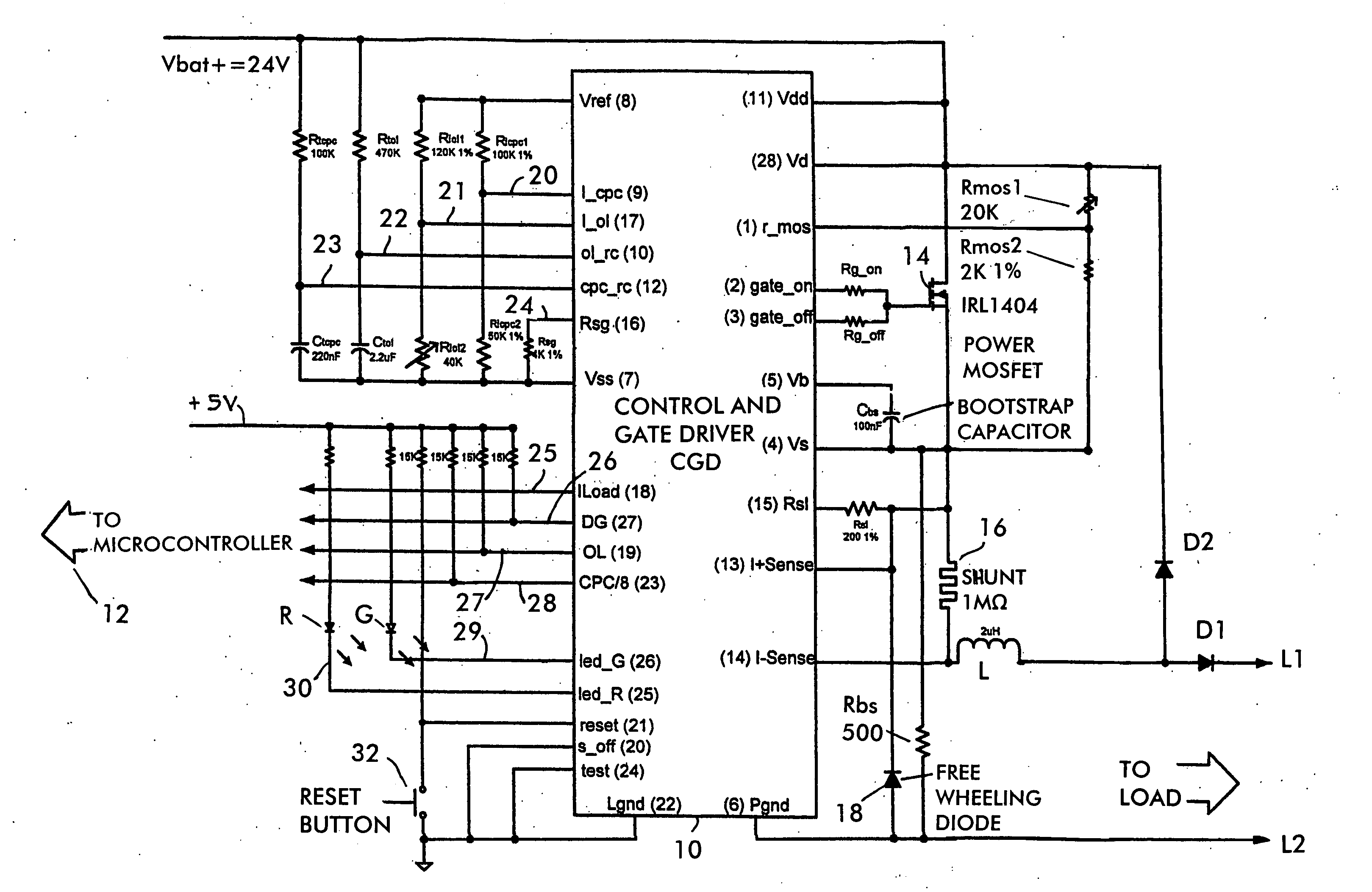
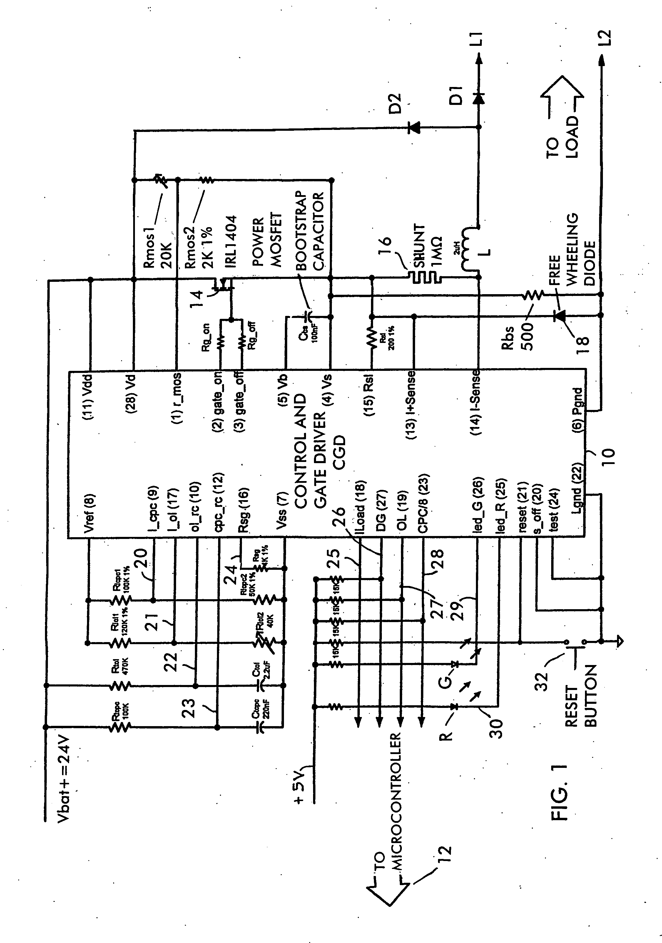
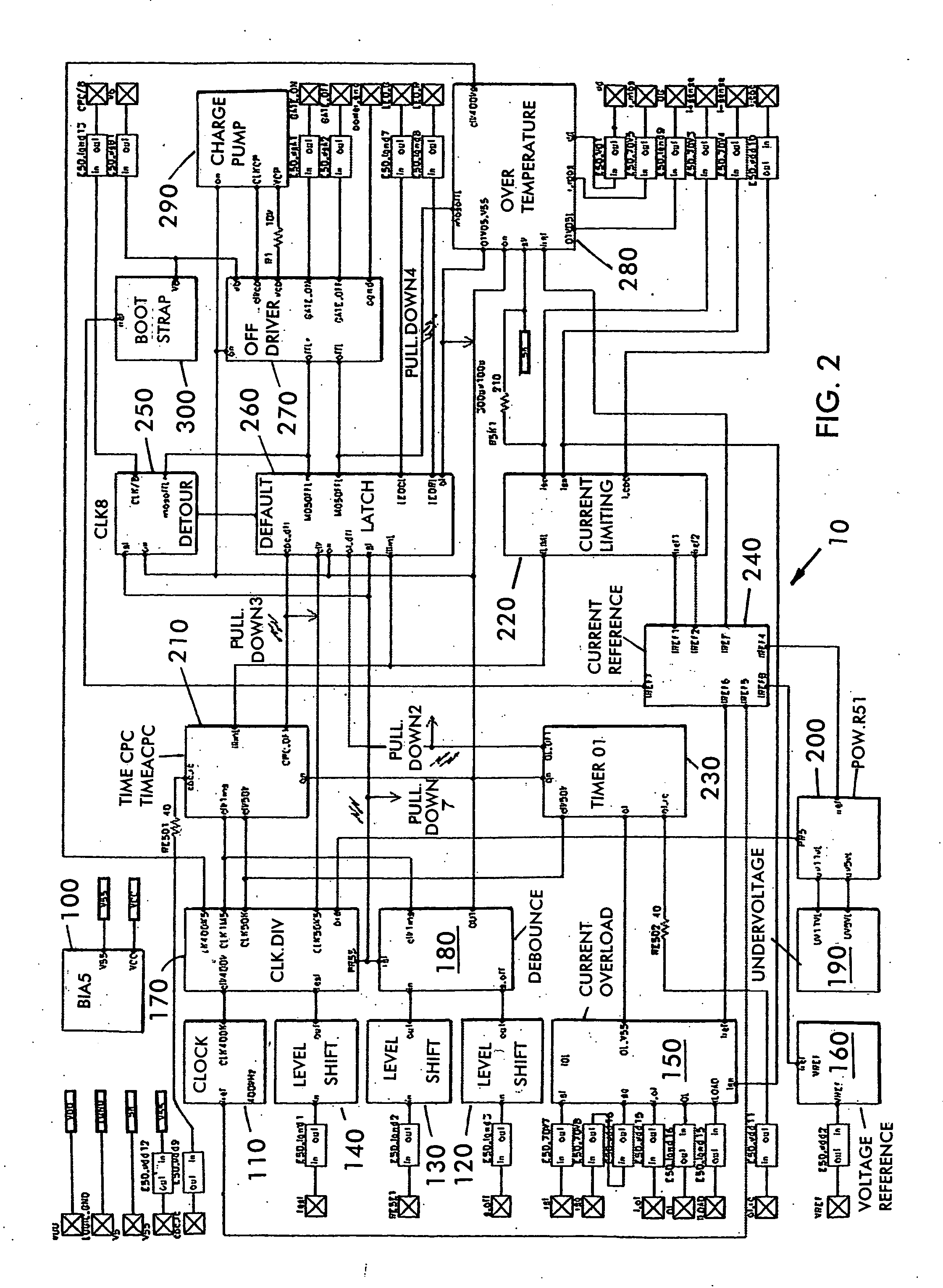
[0025] With reference now to the drawings, FIG. 1 shows the electronic fuse of the present invention. The electronic fuse of the present invention comprises a control and gate driver (CGD) integrated circuit10 which can provide outputs to a monitoring micro-controller as indicated at 12. The integrated circuit 10 includes a number of input and output terminals including a reference voltage Vref, supply voltages Vdd, Vd, Vss and logic ground Lgnd and power ground Pgnd. Also provided are outputs gate-on and gate-off for driving the power MOSFET 14. Terminal Vb is for a bootstrap capacitor Cbs coupled between Vb and Vs, the low side of the semiconductor switch 14. Current sensing inputs I+ sense and I− sense and a terminal Rsi are provided, a resistor Rsi being disposed between input Rsi and I+ sense. A shunt resistor 16 of about 1 mohm (10−3 ohm) is disposed between I+ sense and I− sense. The load is connected in series with an inductance L and diode D1 across points L1 and L2. A free...


PUM


Abstract

An electronic fuse comprising an integrated circuit having a control output terminal coupled to a control electrode of a power semiconductor switching device, the power semiconductor switching device being coupled in series with a load between first and second potentials, the integrated circuit further comprising a current sense input for sensing the current through the power semiconductor switching device, the integrated circuit further comprising a driver circuit for driving the power semi-conductor switching device, the driver circuit being coupled to a current limiting circuit responsive to the sensed current in the power semiconductor switching device, the current limiting circuit controlling the driver circuit whereby if the current through the power semiconductor switching device exceeds a predetermined threshold, the current limiting circuit generates a command to pulse the power semiconductor switching device on and off in a period of pulsed operation to maintain the current in the power semiconductor switching device below a predetermined level, further comprising a first timer circuit for limiting the period of pulsed operation to a preprogrammed first duration and further for controlling the power semiconductor switching device whereby if two commands to pulse the power semiconductor switching device are generated by the current limiting circuit within a duration less than a predetermined second duration, the power semiconductor switching device is turned off.

Description

BACKGROUND OF THE INVENTION [0001] The present invention relates to an electronic fuse. In particular, the present invention relates to an electronic circuit which will act as an electronic fuse for a power semiconductor device in the event of excessive current through the semiconductor device. [0002] U.S. Pat. No. 6,356,423 to Hastings et al. discloses a solid state protection circuit for electrical apparatus in which electrical equipment is safeguarded from damage due to faults by a circuit that provides several levels of protection. A semiconductor switch and a current sensor are placed in series with the electrical equipment. In a first mode of operation when the magnitude of current is less than a first threshold, the semiconductor switch is maintained in a continuous conductive state. In the second mode of operation when the magnitude of current is greater than the first threshold and less than a second threshold, the semiconductor switch is rendered non-conductive after a pre...

Claims


Application Information

Patent Timeline
Patent Type & Authority Applications(United States)
IPC IPC(8): H02H3/02H02H3/087H03K17/082
CPCH02H3/025H03K17/0822H02H3/087
Inventor THIERY, VINCENTNADD, BRUNO C.LEE, CHIK YAM
Owner INFINEON TECH AMERICAS CORP
Why Eureka
Try Eureka