

Organic photosensitive optoelectronic device with an exciton blocking layer
an optoelectronic device and exciton blocking technology, applied in applications, nanoinformatics, transportation and packaging, etc., can solve the problems of significant improvement in the overall performance of solar cells, and achieve the effect of improving the absorption of incident radiation and more efficient photogeneration of charge carriers
- Summary
- Abstract
- Description
- Claims
- Application Information
AI Technical Summary
Benefits of technology
Problems solved by technology
Method used
Image

Examples
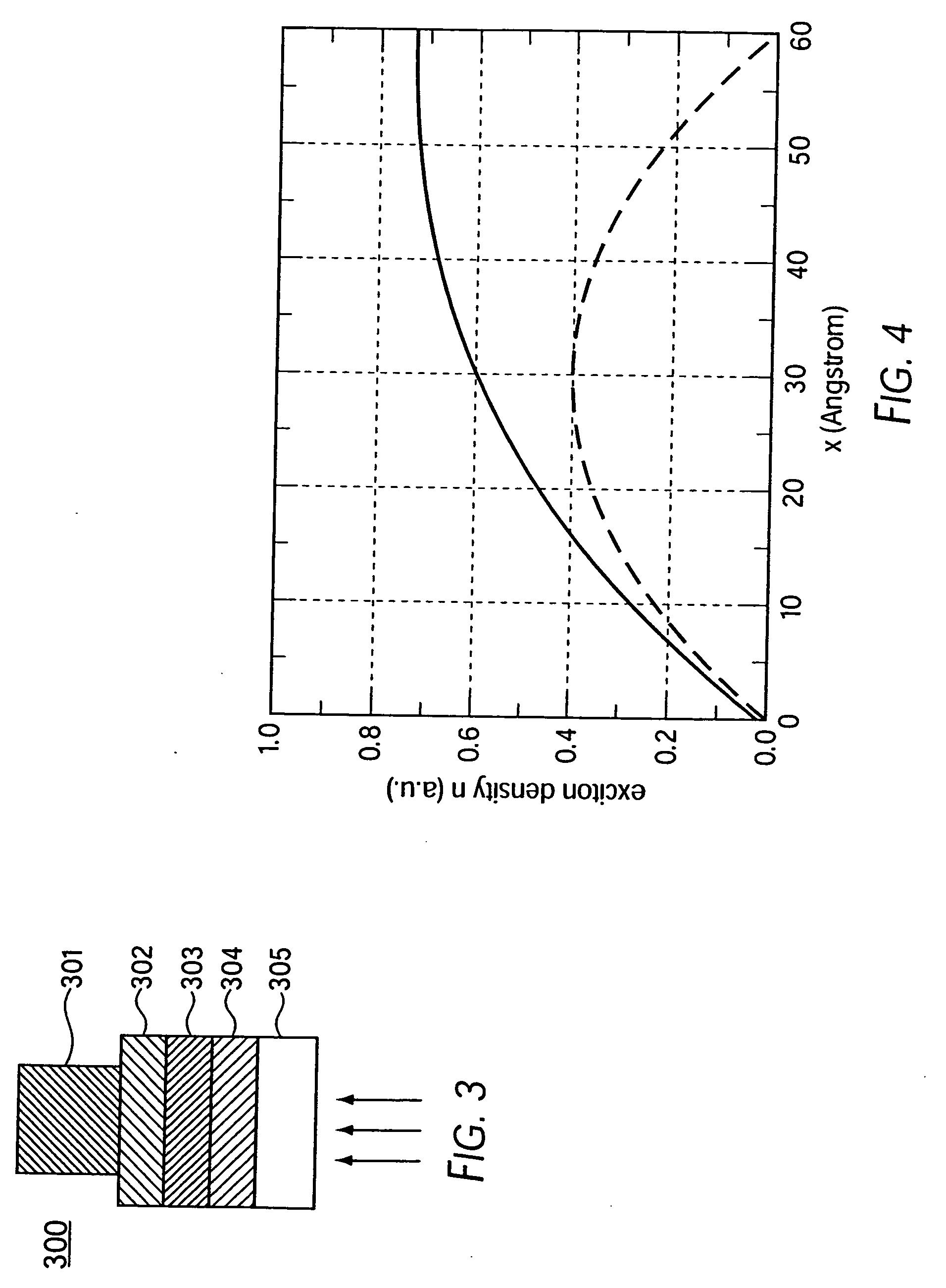
embodiment 300
[0067]FIG. 4 is a theoretical calculation of exciton density as a function of position in a photosensitive organic material under two different boundary conditions for the right interface. Both exciton profiles are for a 60 Å thick layer of an organic photosensitive material, e.g., PTCBI, assuming uniform generation of excitons throughout the film. The uniform generation follows from assuming LD−1, i.e., the absorption length is much greater than the exciton diffusion length. Here, the exciton diffusion length, LD was taken to be 30 Å. The full line assumes an EBL to the right hand side. The dashed line has a quenching interface at the right hand side. In both cases, the left hand interface is the intentional exciton sink (for example the CuPc / PTCBI interface in embodiment 300). In a device in accordance with the present invention such as 300, excitons are purposefully lost at the exciton sink interface where they are converted to pairs of free charge carriers. The much higher value...
embodiment 1000
[0076] Alternatively, it is apparent from measurements of ηINT that an increased ηP can be achieved in a concentrator configuration where photons are forced to make multiple passes through the thin absorbing region. It should be appreciated regarding embodiment 1000 that light incident on a transparent face of the device can generally be reflected once off of an opposite interior reflecting layer and then either absorbed or possibly transmitted back out of the device. Device configurations are described in co-pending U.S. patent application Attorney docket number 10644 / 50501 (“50501 Application”) (incorporated herein by reference) which cause any light admitted to a device to be reflected multiple times to increase absorption efficiency.
embodiment 1100
[0077] A device in accord with the present invention (depicted in FIG. 11) having a reflective Ag layer 1101 with a small aperture on the substrate surface was used to demonstrate this increase in efficiency. Transparent layer 1102, of, for example, glass or plastic, was much wider than the optical coherence length. Transparent anode of degenerately doped ITO 1103 permitted the light to reach electronically active layers 1104. Metallic cathode 1105 reflected unabsorbed light. Concentrated radiation (10 suns at AM1.5) was focused on an aperture in reflective layer 1101 and formed a near normal incidence beam which reflected several times between the cathode and Ag reflecting surface 1101, with each pass suffering additional absorption by a CuPc / PTCBI bilayer adjacent to a BCP EBL (shown collectively as 1104 and like FIG. 2A). FIG. 12 uses the same reference numerals as FIG. 11 to illustrate the circular aperture in reflective layer 1101 since layer 1102 can be seen through the apertu...
PUM
| Property | Measurement | Unit |
|---|---|---|
| semi-transparent | aaaaa | aaaaa |
| LUMO-HOMO separation | aaaaa | aaaaa |
| LUMO-HOMO separation | aaaaa | aaaaa |
Abstract
Description
Claims
Application Information