Indium oxide conductive film structures

a technology of indium oxide and conductive film, applied in the direction of semiconductor devices, electrical devices, transistors, etc., can solve the problem of much longer memory retention time of these devices than the prior art structur

Active Publication Date: 2005-06-23
SHARP KK
View PDF8 Cites 15 Cited by
  • Summary
  • Abstract
  • Description
  • Claims
  • Application Information

AI Technical Summary

Problems solved by technology

Therefore, the memory retention time associated with these devices is much longer than the prior art structures.

Method used


Image

  • Indium oxide conductive film structures
  • Indium oxide conductive film structures
  • Indium oxide conductive film structures

Examples


Embodiment Construction

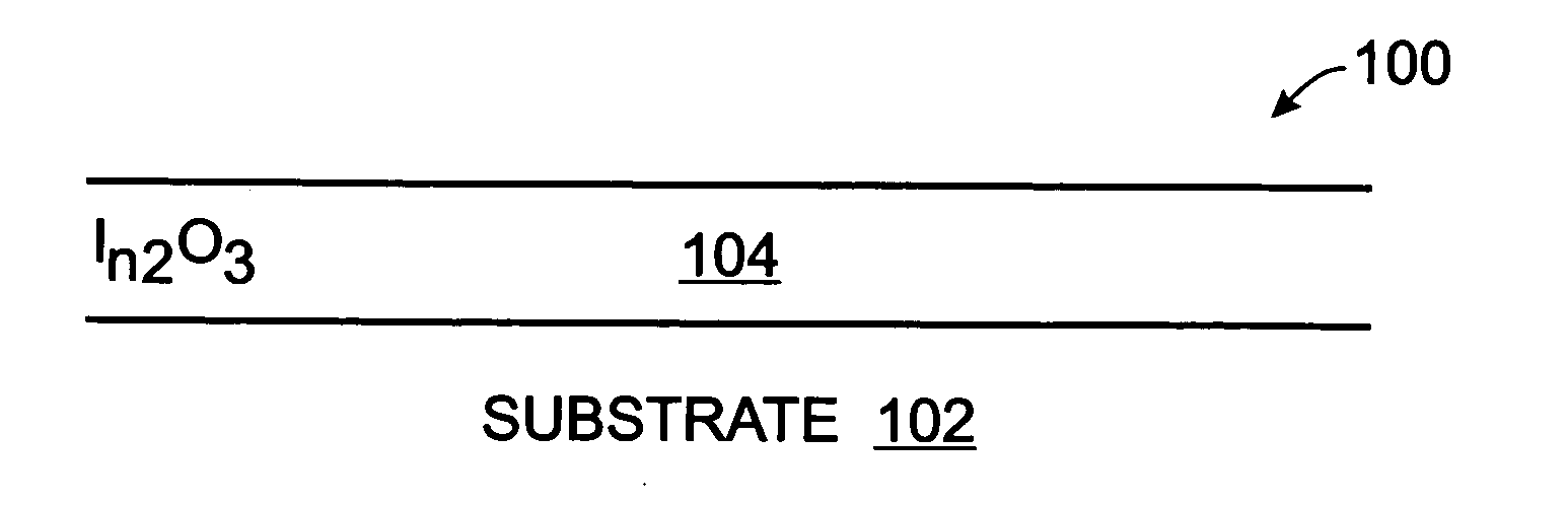
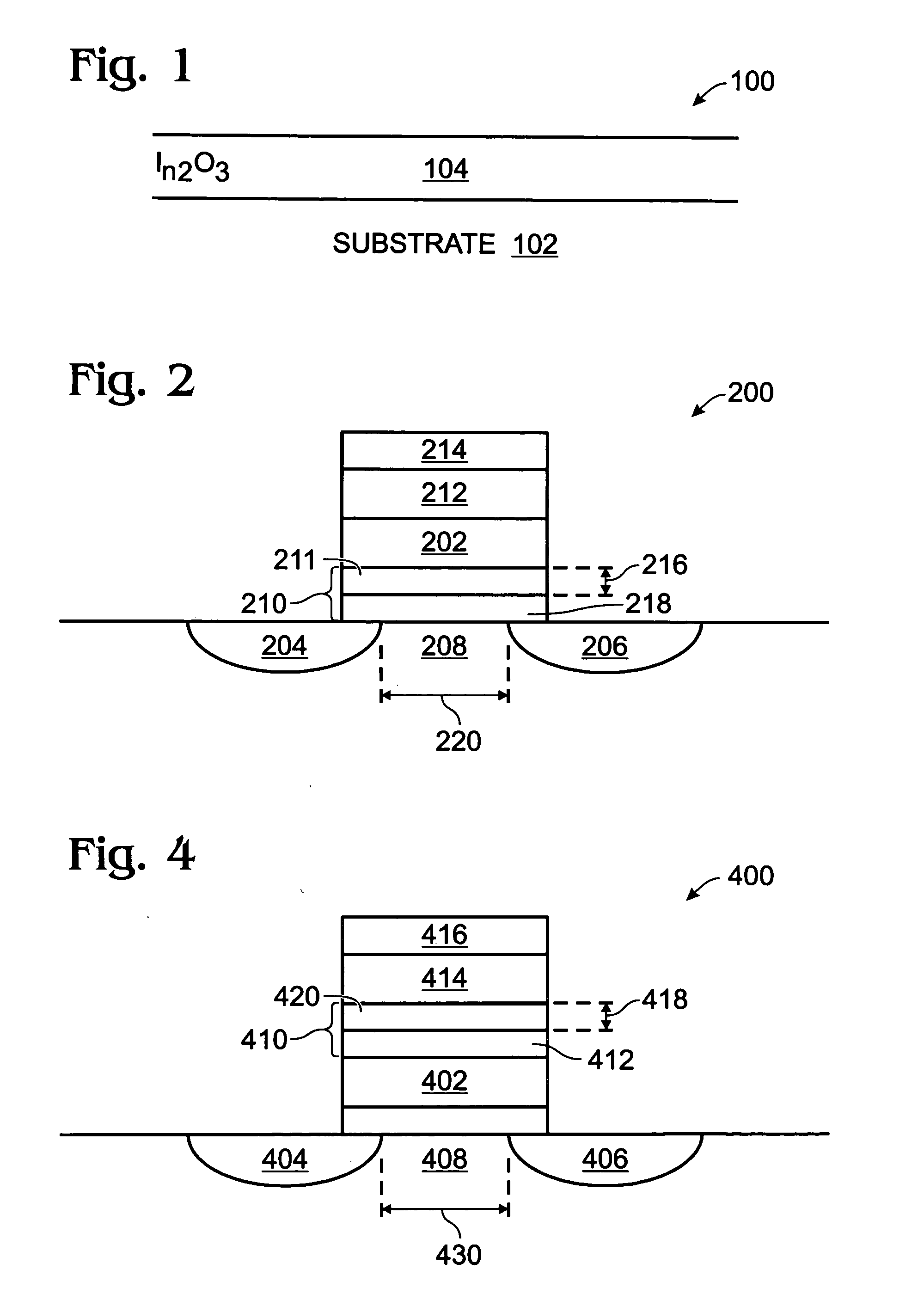
[0032]FIG. 1 is a partial cross-sectional view of the present invention indium oxide (In2O3 ) film structure. The film structure 100 comprises a substrate 102 and an In2O3 film 104 overlying the substrate 102, having a resistivity in the range of 260 to 800 ohm-cm. The substrate 102 can be a material such as platinum (Pt), iridium (Ir), other noble metals, silicon (Si), high-k oxides, or silicon dioxide (SiO2).

[0033]FIG. 2 is a partial cross-sectional view of the present invention 1T memory device using an In2O3 film as a gate insulator. The device 200 comprises a CMOS transistor gate 202, source 204, drain 206, and channel region 208. A gate insulator 210 is formed from an In2O3 thin film 211, interposed between the channel region 208 and the gate 202. The In2O3 film 211 has a resistivity in the range of 260 to 800 ohm-cm. A memory cell film 212 overlies the gate electrode 202. A top electrode 214 overlies the memory cell film 212.

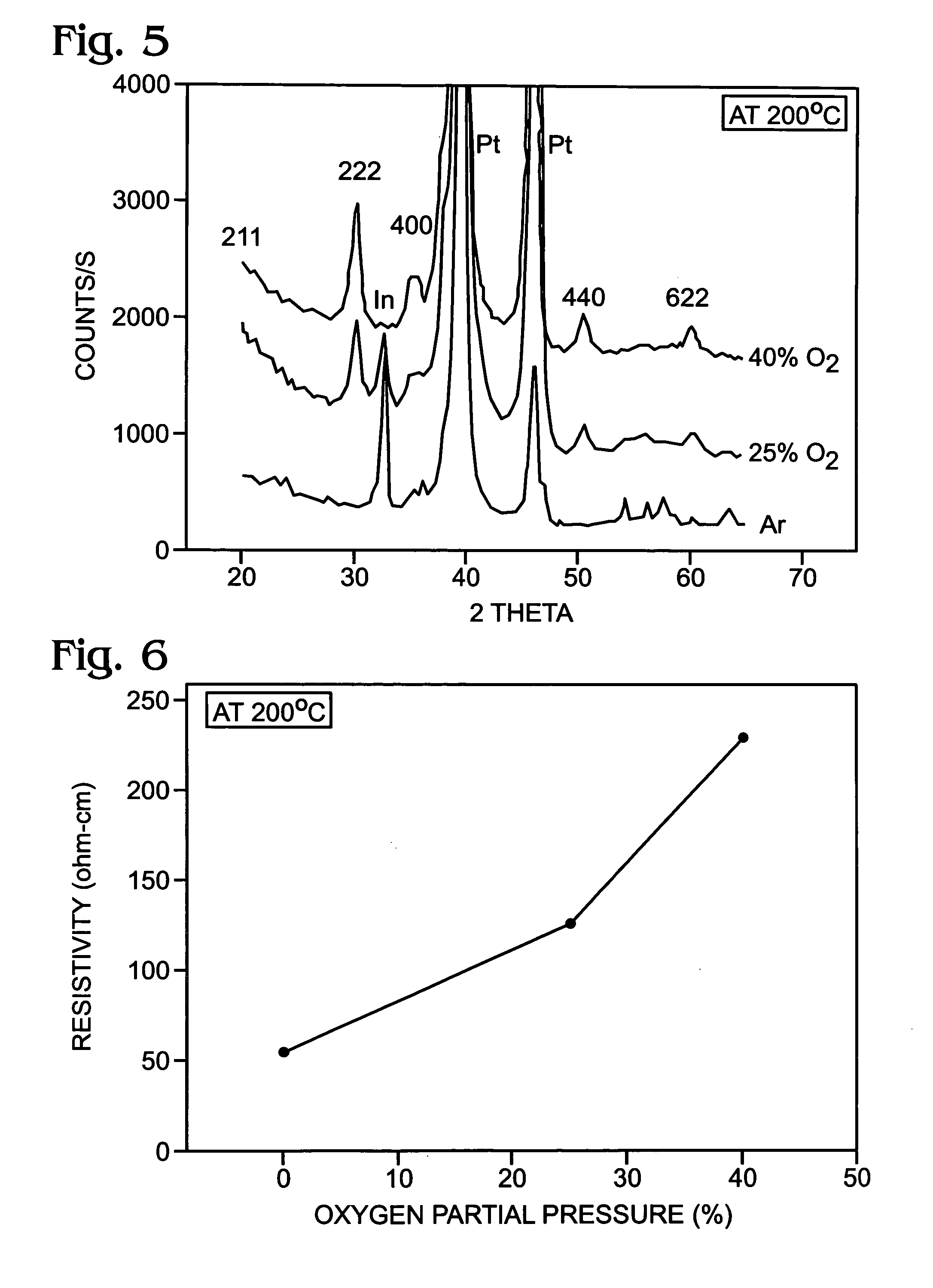
[0034] The In2O3 thin film 211 includes crystals ...


PUM

PropertyMeasurementUnit
grain sizeaaaaaaaaaa
thicknessaaaaaaaaaa
gate channel lengthaaaaaaaaaa

Abstract

One-transistor ferroelectric memory devices using an indium oxide film (In2O3), an In2O3 film structure, and corresponding fabrication methods have been provided. The method for controlling resistivity in an In2O3 film comprises: depositing an In film using a PVD process, typically with a power in the range of 200 to 300 watts; forming a film including In overlying a substrate material; simultaneously (with the formation of the In-including film) heating the substrate material, typically the substrate is heated to a temperature in the range of 20 to 200 degrees C.; following the formation of the In-including film, post-annealing, typically in an O2 atmosphere; and, in response to the post-annealing: forming an In2O3 film; and, controlling the resistivity in the In2O3 film. For example, the resistivity can be controlled in the range of 260 to 800 ohm-cm.

Description

RELATED APPLICATIONS [0001] This application is a Divisional of a pending patent application entitled, INDIUM OXIDE CONDUCTIVE FILM, invented by Li et al., Ser. No. 10 / 741,803, filed Dec. 18, 2003.BACKGROUND OF THE INVENTION [0002] 1. Field of the Invention [0003] This invention generally relates to integrated circuit (IC) fabrication and, more particularly, to an indium oxide (In2O3) film with a controlled resistivity for use in ferroelectric memory devices, and a method for fabricating the same. [0004] 2. Description of the Related Art [0005] One-transistor (1T) ferroelectric memory devices are conventionally made with MFMOS (Metal, Ferroelectrics, Metal, Oxide and Silicon) or MFOS (Metal, Ferroelectrics, Oxide, and Silicon). The retention properties of 1T ferroelectric memories present a considerable technical challenge, due to the generation of a depolarization field once the device has been programmed. Three possible mechanisms may be responsible for the poor retention of 1T fe...

Claims


Application Information

Patent Timeline
Patent Type & Authority Applications(United States)
IPC IPC(8): H01L21/28H01L21/316H01L29/51H01L29/78
CPCH01L21/28185H01L21/28194H01L21/28273H01L29/78391H01L21/31604H01L29/513H01L29/517H01L21/28291H01L29/40114H01L29/40111H01L21/02266H01L21/02197H01L21/02112H01L21/02337
Inventor LI, TINGKAIHSU, SHENG TENG
Owner SHARP KK
Why Eureka
Try Eureka