Hydrogen free integration of high-k gate dielectrics

a technology of high-k gate dielectrics and hydrogen-free integration, which is applied in the field of semiconductor device fabrication, can solve the problems of increasing the thickness of gate dielectrics, reducing the efficiency of the device, and reducing the amount of hydrogen, so as to facilitate the device scaling

Active Publication Date: 2005-06-23
TEXAS INSTR INC
View PDF6 Cites 3 Cited by
  • Summary
  • Abstract
  • Description
  • Claims
  • Application Information

AI Technical Summary

Benefits of technology

[0021] The present invention pertains to forming a transistor in the absence of hydrogen, or in the presence of a significantly reduced amount of hydrogen. In this manner, a high-k material can be utilized to form a gate dielectric layer in the transistor and facilitate device scaling while mitigating defects that can be introduced into the high-k material by the presence of hydrogen and / or hydrogen containing compounds.

Problems solved by technology

Recently, however, electrical and physical limitations have been reached in the thickness of gate dielectrics, particularly those formed of silicon dioxide.
However, making the gate dielectric layer 30 thinner can have undesirable results, particularly where the gate dielectric 30 is SiO2.
While such a high-k dielectric layer 30′ assists in mitigating of some of the issues encountered with device scaling, other issues may persist, however.
For example, hydrogen and / or hydrogen containing compounds are commonly utilized in many of the stages of semiconductor fabrication, and hydrogen can react with high-k dielectric materials such as hafnium oxide and adversely affect the construction and / or electrical properties thereof.
Atomic hydrogen is a strong etchant of silicon and silicon based compounds, and thus may undesirably reduce many high-k dielectric materials.
Such defects 50′ can counteract or negate some of the positive aspects of high-k materials by potentially reducing the electrical thickness of the high-k material 30′ and increasing the leakage path through the high-k dielectric at these defects, thus leading to the aforementioned issues at the contaminated locations 50′.
Further, such defects 50′ disrupt the uniformity of the high-k dielectric material 30′ which can adversely affect the operation of the transistor 6′ by, among other things, disrupting electromagnetic fields that are developed between the gate electrode 32′ and the source 24a′, drain 24b′ and / or channel 26′ regions of the transistor when a bias voltage is applied to the gate electrode 32′.

Method used


Image

  • Hydrogen free integration of high-k gate dielectrics
  • Hydrogen free integration of high-k gate dielectrics
  • Hydrogen free integration of high-k gate dielectrics

Examples


Embodiment Construction

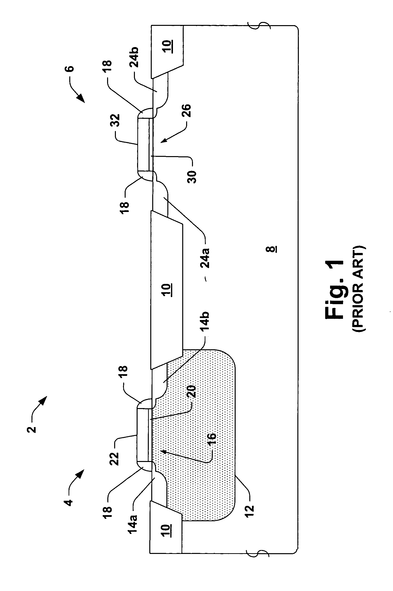
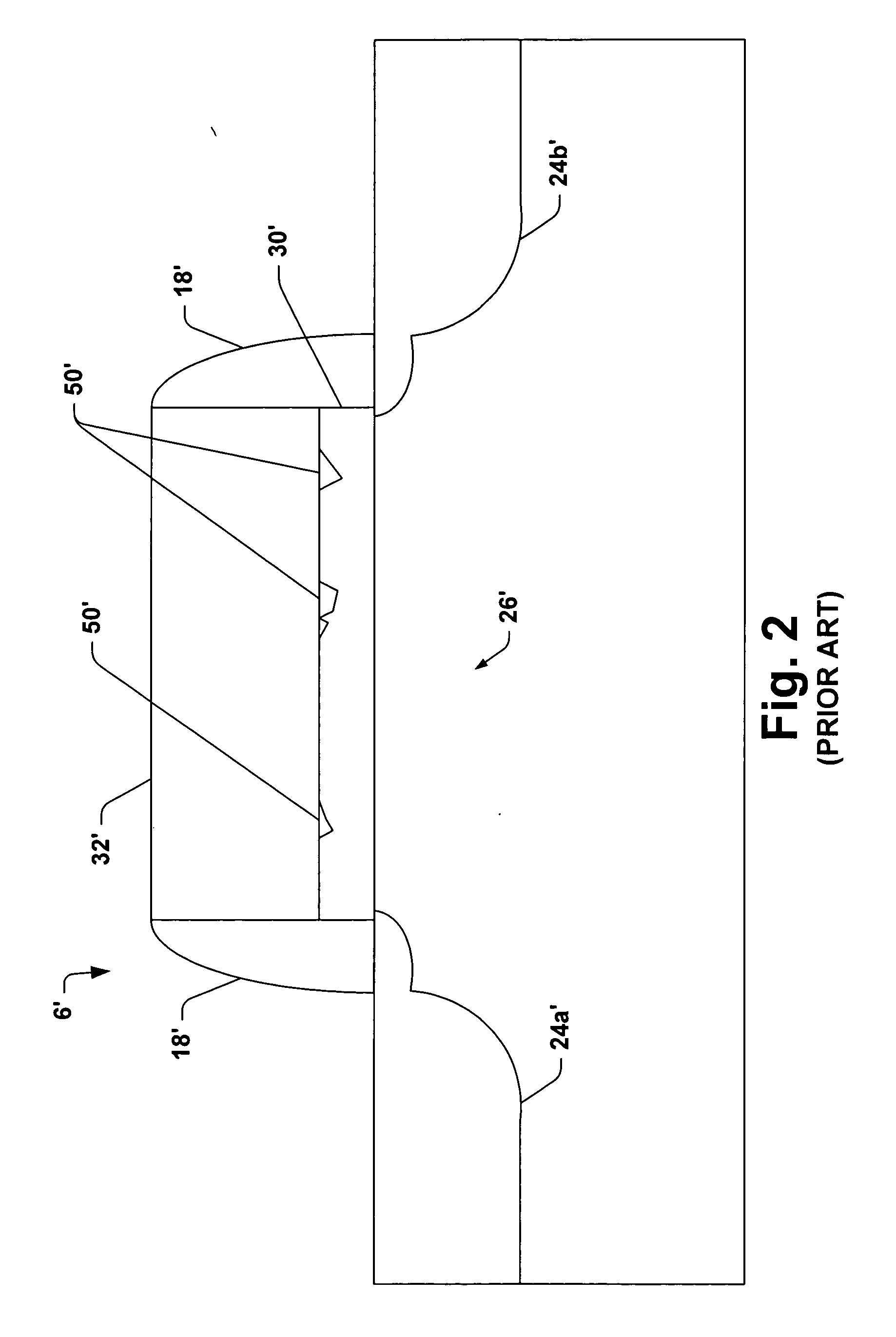
[0026] One or more aspects of the present invention are described with reference to the drawings, wherein like reference numerals are generally utilized to refer to like elements throughout, and wherein the various structures are not necessarily drawn to scale. In the following description, for purposes of explanation, numerous specific details are set forth in order to provide a thorough understanding of one or more aspects of the present invention. It may be evident, however, that one or more aspects of the present invention may be practiced with a lesser degree of these specific details. In other instances, well-known structures and devices are shown in block diagram form in order to facilitate describing one or more aspects of the present invention.

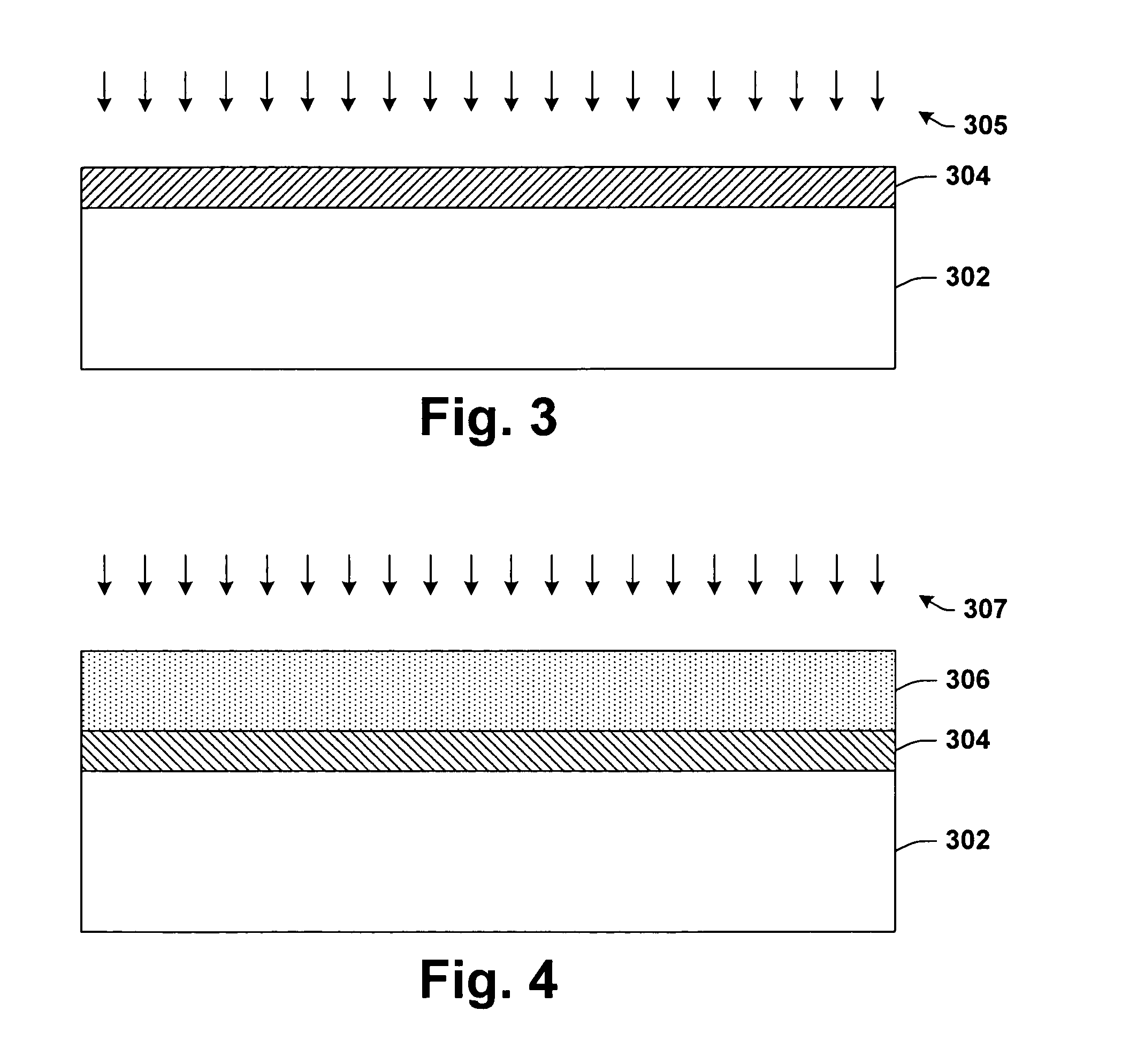
[0027] The present invention pertains to forming a transistor in the absence of or in the presence of a significantly reduced amount of hydrogen. In this manner, a high-k material can be utilized to form a gate dielectric layer in th...


PUM


Abstract

The present invention pertains to forming a transistor in the absence of hydrogen, or in the presence of a significantly reduced amount of hydrogen. In this manner, a high-k material can be utilized to form a gate dielectric layer in the transistor and facilitate device scaling while mitigating defects that can be introduced into the high-k material by the presence of hydrogen and/or hydrogen containing compounds.

Description

RELATED APPLICATIONS [0001] This application is related to U.S. Patent Application Serial No.______, (TI Attorney Docket No. TI-35223), filed on Dec. 22, 2003, entitled HYDROGEN FREE FORMATION OF GATE ELECTRODES, wherein the entirety of this application is hereby incorporated by reference as if fully set forth herein. FIELD OF INVENTION [0002] The present invention relates generally to semiconductor processing, and more particularly to fabricating semiconductor devices employing high-k dielectric materials in the absence of or in a significantly reduced amount of hydrogen and / or hydrogen containing compounds. BACKGROUND OF THE INVENTION [0003] Field effect transistors (FETs) are widely used in the electronics industry for switching, amplification, filtering, and / or other tasks related to both analog and digital electrical signals. Most common among these are MOSFETs, wherein a metal or (doped) polysilicon gate contact or electrode is energized to create an electric field in an under...

Claims


Application Information

Patent Timeline
Patent Type & Authority Applications(United States)
IPC IPC(8): H01L21/28H01L21/311H01L21/314H01L21/316H01L21/318H01L21/336H01L29/51
CPCH01L21/02164Y10S438/954H01L21/022H01L21/02271H01L21/02274H01L21/28194H01L21/31111H01L21/3144H01L21/3145H01L21/31608H01L21/3185H01L29/517H01L29/518H01L29/665H01L29/6656H01L29/6659Y10S438/91H01L21/0217
Inventor COLOMBO, LUIGICHAMBERS, JAMES J.VISOKAY, MARK R.
Owner TEXAS INSTR INC
Why Eureka
Try Eureka