Metal insulator metal (MIM) capacitor fabrication with sidewall spacers and aluminum cap (ALCAP) top electrode

a metal insulator and capacitor technology, applied in capacitors, semiconductor devices, semiconductor/solid-state device details, etc., can solve the problems of capacitor dielectric layer being “overcharged” and/or blowing, and achieve the effect of facilitating device scaling, reducing adverse effects, and reducing the number of capacitors

Active Publication Date: 2006-02-02
TEXAS INSTR INC
View PDF12 Cites 53 Cited by
  • Summary
  • Abstract
  • Description
  • Claims
  • Application Information

AI Technical Summary

Benefits of technology

[0008] The present invention relates to forming a MIM (metal insulator metal) capacitor in a manner that facilitates device scaling while mitigating adverse effects associated with copper diffusion. In particular, sidewall spacers are formed along respective edges of a layer bottom electrode material, a layer of capacitor dielectric material and at least some of an edge of a layer of top electrode material. The sidewall spacers are formed from a dielectric or non-conductive material to a thickness sufficient to mitigate undesirable electron flow and, as such, the spacers serve to mitigate leakage or “shorting” currents that can develop between the bottom electrode, dielectric and top electrode layers. An excess of electron leakage current can cause the capacitor dielectric layer to become “overcharged” and / or blow. Leakage current is more likely to occur at corners of the layers where electric fields are enhanced. Accordingly, forming the sidewall spacers at the edges / corners of the layer addresses leakage current problems at the most likely “failure spots”. Further, a layer of aluminum capping (ALCAP) material is utilized as at least part of a top electrode, while a metal in a topmost metallization layer is utilized as at least part of a bottom electrode. In this manner, resulting devices are formed as away from the silicon substrate as possible. This distance away from the substrate is advantageous for RF applications in that the quality factor (a figure of merit for RF performance) increases with distance for the “lossy” substrate. This is particularly true where the substrate comprises silicon.

Problems solved by technology

An excess of electron leakage current can cause the capacitor dielectric layer to become “overcharged” and / or blow.

Method used


Image

  • Metal insulator metal (MIM) capacitor fabrication with sidewall spacers and aluminum cap (ALCAP) top electrode
  • Metal insulator metal (MIM) capacitor fabrication with sidewall spacers and aluminum cap (ALCAP) top electrode
  • Metal insulator metal (MIM) capacitor fabrication with sidewall spacers and aluminum cap (ALCAP) top electrode

Examples


Embodiment Construction

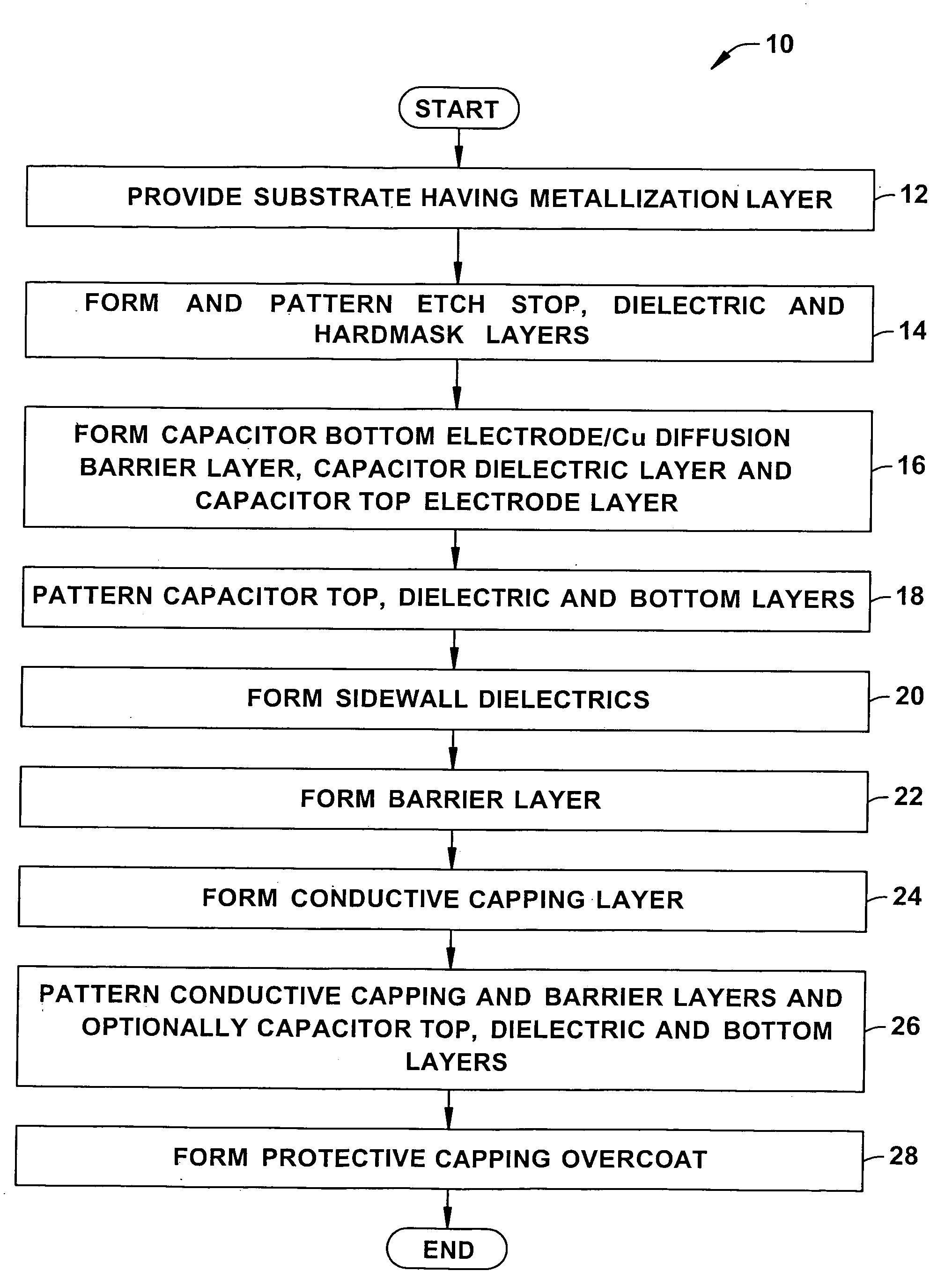
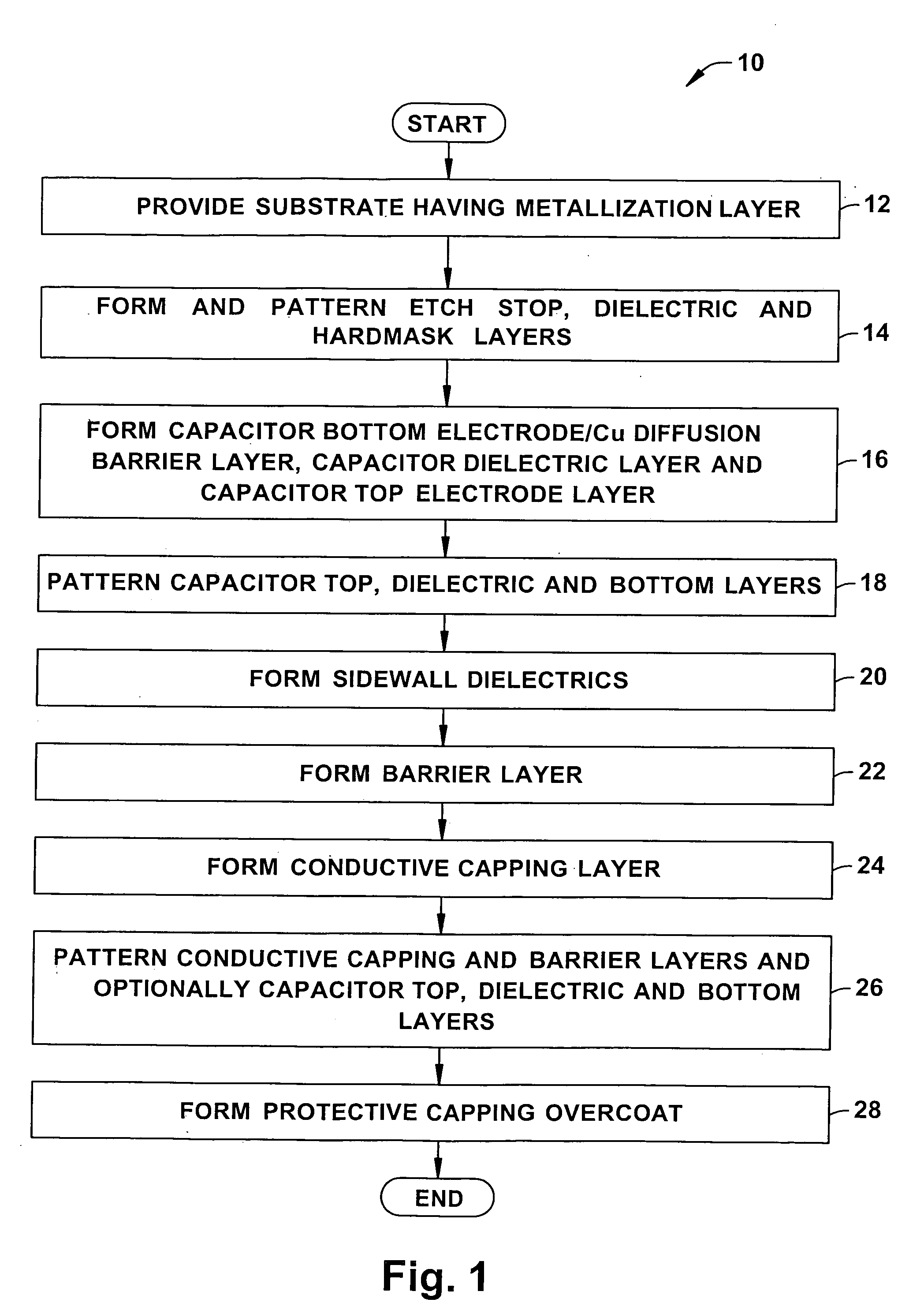
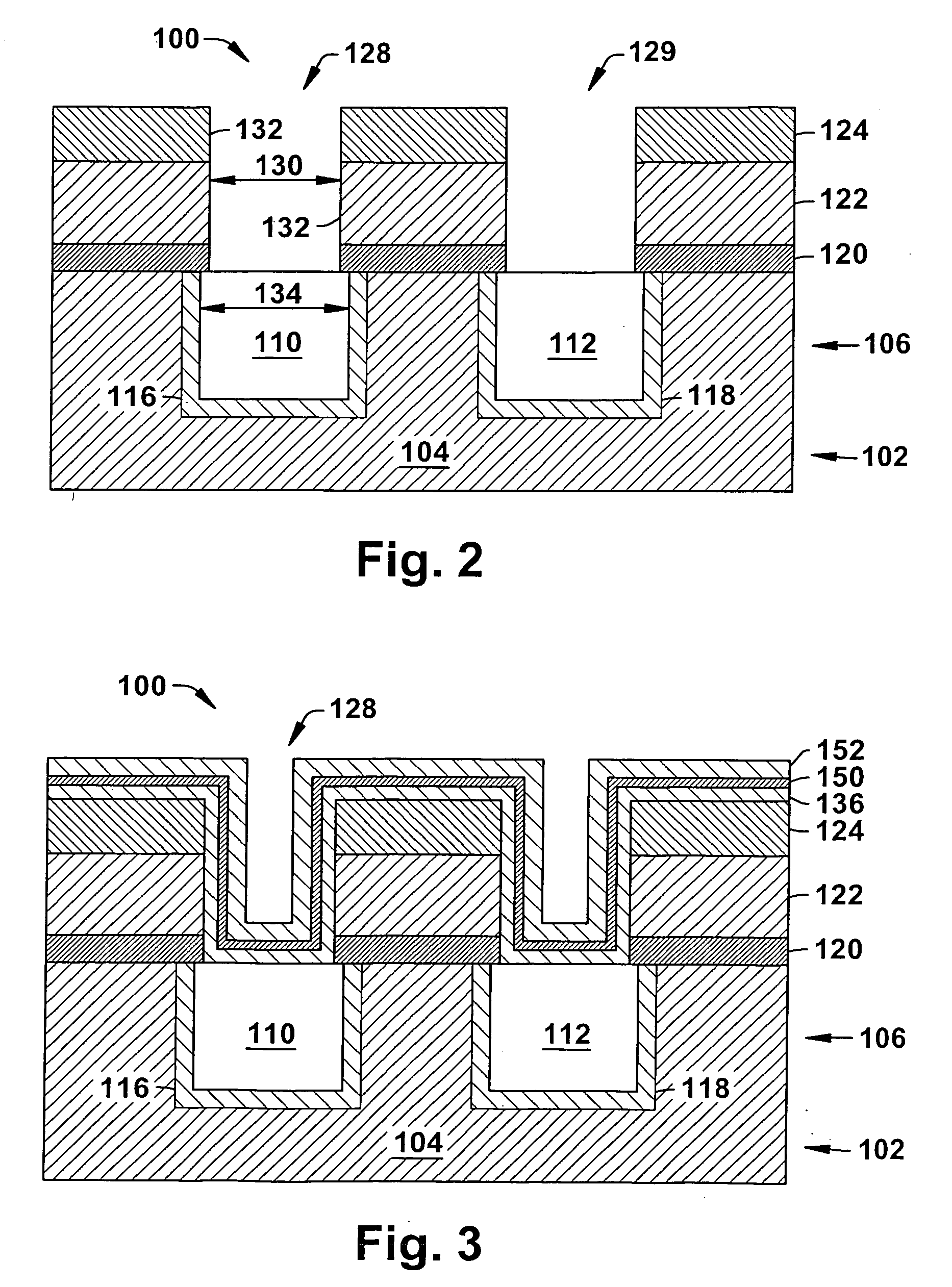
[0019] One or more aspects of the present invention are described with reference to the drawings, wherein like reference numerals are generally utilized to refer to like elements throughout, and wherein the various structures are not necessarily drawn to scale. It will be appreciated that where like acts, events, elements, layers, structures, etc. are reproduced, subsequent (redundant) discussions of the same may be omitted for the sake of brevity. In the following description, for purposes of explanation, numerous specific details are set forth in order to provide a thorough understanding of one or more aspects of the present invention. It may be evident, however, to one of ordinary skill in the art that one or more aspects of the present invention may be practiced with a lesser degree of these specific details. In other instances, known structures are shown in diagrammatic form in order to facilitate describing one or more aspects of the present invention.

[0020] The present inven...


PUM

PropertyMeasurementUnit
thicknessaaaaaaaaaa
thicknessaaaaaaaaaa
thicknessaaaaaaaaaa

Abstract

A method (10) of forming a MIM (metal insulator metal) capacitor is disclosed whereby adverse affects associated with copper diffusion are mitigated even as the capacitor is scaled down. A sidewall spacer (156) is formed against an edge (137) of a layer of bottom electrode/copper diffusion barrier material (136), an edge (151) of a layer of capacitor dielectric material (150) and at least some of an edge (153) of a layer of top electrode material. The sidewall spacer (156) is dielectric or non-conductive and mitigates “shorting” currents that can develop between the plates as a result of copper diffusion. Bottom electrode diffusion barrier material (136) mitigates copper diffusion and/or copper drift, thereby reducing the likelihood of premature device failure.

Description

FIELD OF INVENTION [0001] The present invention relates generally to semiconductor devices, and more particularly to fabricating a MIM capacitor with sidewall spacers and an aluminum capping (ALCAP) layer serving as a top electrode. BACKGROUND OF THE INVENTION [0002] In the manufacture of semiconductor products such as integrated circuits, individual electrical devices are formed on or in a semiconductor substrate, and are thereafter interconnected to form circuits. Interconnection of these devices is typically accomplished by forming a multi-level interconnect network in and through one or more dielectric or non-conductive layers that are formed over the electrical devices to electrically isolate the devices from one another. A conductive material, such as copper, is deposited into vias and / or trenches formed within these dielectric layers to connect the devices and thereby establish the multi-level interconnect network. [0003] MIM (metal insulator metal) capacitors are semiconduct...

Claims


Application Information

Patent Timeline
Patent Type & Authority Applications(United States)
IPC IPC(8): H01L21/8242H01L21/20
CPCH01L21/76834H01L28/91H01L28/57H01L23/5223H01L2924/0002H01L2924/00
Inventor CRENSHAW, DARIUS L.WILLIAMS, BYRON L.TSAO, ALWINSHICHIJO, HISASHIPAPA RAO, SATYAVOLU S.BRENNAN, KENNETH D.LYTLE, STEVEN A.
Owner TEXAS INSTR INC
Why Eureka
Try Eureka