Data control circuit for DDR SDRAM controller

a data control circuit and controller technology, applied in the field of data control circuits, can solve the problems of ddr sdram controllers that cannot actively cope with the change of the operating speed of ddr sdram or the whole system, and complicate the whole system, and achieve the effect of stable reading/writing operation of ddr sdram data

Inactive Publication Date: 2005-06-23
SAMSUNG ELECTRONICS CO LTD
View PDF6 Cites 39 Cited by
  • Summary
  • Abstract
  • Description
  • Claims
  • Application Information

AI Technical Summary

Benefits of technology

[0018] An aspect of the present invention is to solve the above and / or other problems and disadvantages and to provide at least the advantages described below. Accordingly, an aspect of the present invention is to provide a data control circuit for a double data rate (DDR) synchronous dynamic random-access memory (SDRAM) that secures a stable reading / writing operation of DDR SDRAM data by internally generating and using a data strobe signal located in the center part of valid data.

Problems solved by technology

Accordingly, the flip-flop of the read data control circuit may capture invalid data, thereby causing the whole system not to operate.
Also, when using the buffer having a fixed delay time as in the conventional method, the DDR SDRAM controller cannot actively cope with the change of the operating speed of the DDR SDRAM or the whole system, and thus an addition circuit composed of buffers having diverse delay times to select a proper delay time according to the operating speed is required.
However, this complicates the whole system and causes an additional cost.
Also, even if the circuit for selecting the delay time is additionally employed, the phase of the clock may be changed due to environmental factors such as temperature, manufacturing process, and external operation voltage, and this phase change causes the valid data not to be normally captured.
As the DDR SDRAM operates at high speed, the valid data window of the DDR SDRAM becomes narrower, and this exacerbates the problems described above.

Method used


Image

  • Data control circuit for DDR SDRAM controller
  • Data control circuit for DDR SDRAM controller
  • Data control circuit for DDR SDRAM controller

Examples


Embodiment Construction

[0040] Reference will now be made in detail to the embodiments of the present invention, examples of which are illustrated in the accompanying drawings, wherein like reference numerals refer to the like elements throughout. The embodiments are described below to explain embodiments of the present invention by referring to the figures.

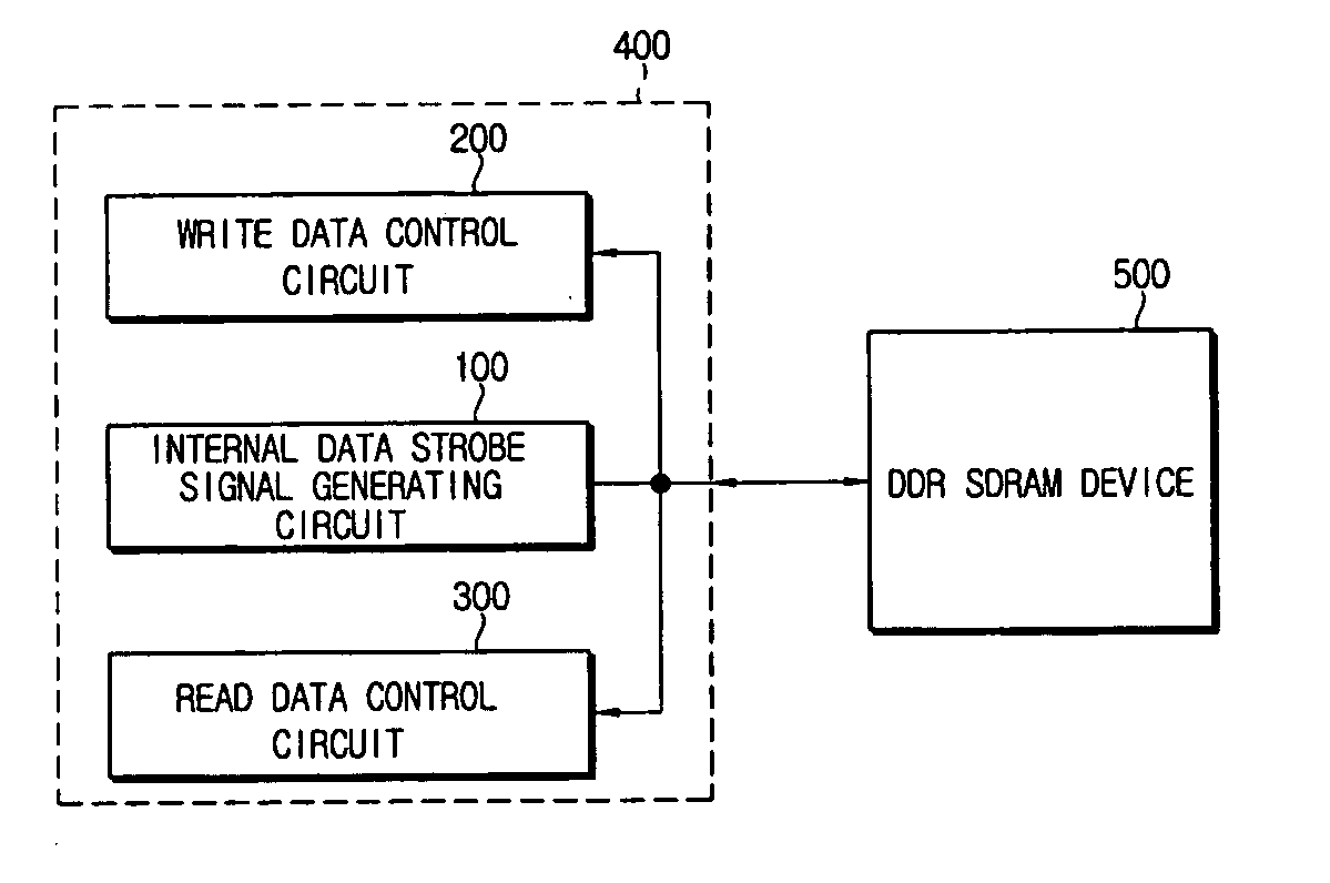
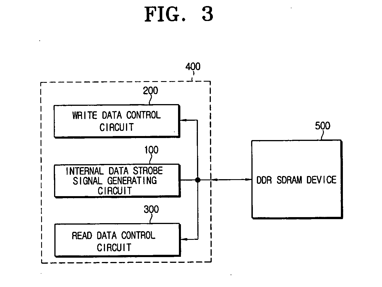
[0041]FIG. 3 is a block diagram illustrating the construction of a data control circuit for a DDR SDRAM 500 according to an embodiment of the present invention. Referring to FIG. 3, the data control circuit 400 for a DDR SDRAM according to an embodiment of the present invention comprises a write data control circuit 200, a read data control circuit 300, and an internal data strobe signal generating circuit 100.

[0042] The internal data strobe signal generating circuit 100 generates and outputs an internal data strobe signal DQS_IN where a rising edge of which is located in a center part of valid data in order to secure a stable reading / writing operatio...


PUM


Abstract

A data control circuit for a double data rate (DDR) synchronous dynamic random-access memory (SDRAM) that secures a stable reading/writing operation of DDR SDRAM data by generating an actively controllable internal data strobe signal. The data control circuit includes an internal data strobe signal generating circuit generating and outputting an internal data strobe signal a rising edge of which is located in a center part of valid DDR SDRAM data; a read data control circuit for receiving the internal data strobe signal, generated from the internal data strobe signal generating circuit as a clock input, dividing captured data into even data and odd data, and transmitting the even data and the odd data to a system bus; and a write data control circuit transmitting the internal data strobe signal input from the internal data strobe signal generating circuit to a DDR SDRAM device as a data strobe signal.

Description

CROSS-REFERENCE TO RELATED APPLICATIONS [0001] This application claims the benefit of Korean Application No. 2003-93226, filed Dec. 18, 2003, in the Korean Intellectual Property Office, the disclosure of which is incorporated herein by reference. BACKGROUND OF THE INVENTION [0002] 1. Field of the Invention [0003] The present invention relates to a data control circuit for a double data rate (DDR) synchronous dynamic random-access memory (SDRAM) controller. More particularly, the present invention relates to a data control circuit for a DDR SDRAM controller which can stably perform a data reading / writing operation by actively controlling a data strobe signal during a data transmission / reception between a DDR SDRAM and the DDR SDRAM controller. [0004] 2. Description of the Related Art [0005] As is well known, in order to increase the data access speed of a DRAM as high as a static random access memory (SRAM) and to obtain a high data bandwidth by a high clock frequency, a synchronous ...

Claims


Application Information

Patent Timeline
Patent Type & Authority Applications(United States)
IPC IPC(8): G11C11/40G06F13/00G06F13/16
CPCG06F13/1689G11C11/4076G11C11/4096
Inventor KOO, TAE-WOON
Owner SAMSUNG ELECTRONICS CO LTD
Why Eureka
Try Eureka