Method and apparatus for test and repair of marginally functional SRAM cells

a technology of marginally functional sram cells and repair methods, applied in the field of repair of embedded memory, can solve the problems of loss of contents, failure in the field under normal operating conditions, and volatile sram cells

Inactive Publication Date: 2005-06-23
IBM CORP
View PDF15 Cites 25 Cited by
  • Summary
  • Abstract
  • Description
  • Claims
  • Application Information

AI Technical Summary

Benefits of technology

[0019] To achieve these and other objects and in view of its purposes, the present invention provides a method of manufacturing a device having embedded memory including a plurality of memory cells. A first test stress is applied to selected cells of the plurality of memory cells with a built-in self test. At least one weak memory cell is identified. The at least one weak memory cell is repaired. A second test stress that is less than the first test stress is applied to the selected cells and the repaired cells with the built-in self test.

Problems solved by technology

Nevertheless, a SRAM cell is still volatile: it will lose its contents when the power is switched off (in contrast to a read-only memory or “ROM” cell).
They might pass initial testing, but then fail in the field under normal operating conditions which are slightly different from the conditions that are present during the initial testing.
Even if cells are tested at operational speed, there might be a cell that is right on the edge of failure and can fail in the field after it is shipped to the customer and while the customer is using it in the customer's application.
When SRAM cells fail in the field, the failure creates a “shipped product quality level” or SPQL problem.
If the SPQL number gets too high, the customers are dissatisfied.
Even though the supplier of the memory cells can give the customer a new part, the customer may have experienced unnecessary delays.
Although IC manufacturers strive to make chips with minimum defects, as a practical matter defects still occur for various reasons.
Embedded memories are increasingly susceptible to such defects as the density and quantity of memory on ICs increases.
The patent shows a simple BIST that does not have the flexibility to test the memory in a harder or easier manner.
If the testing procedure waits long enough (for example, two or three milliseconds), thereby inserting a pause, the system will find a fail.
But the customer has to wait every time the system is powered up for the entire sequence to complete.

Method used


Image

  • Method and apparatus for test and repair of marginally functional SRAM cells
  • Method and apparatus for test and repair of marginally functional SRAM cells
  • Method and apparatus for test and repair of marginally functional SRAM cells

Examples


Embodiment Construction

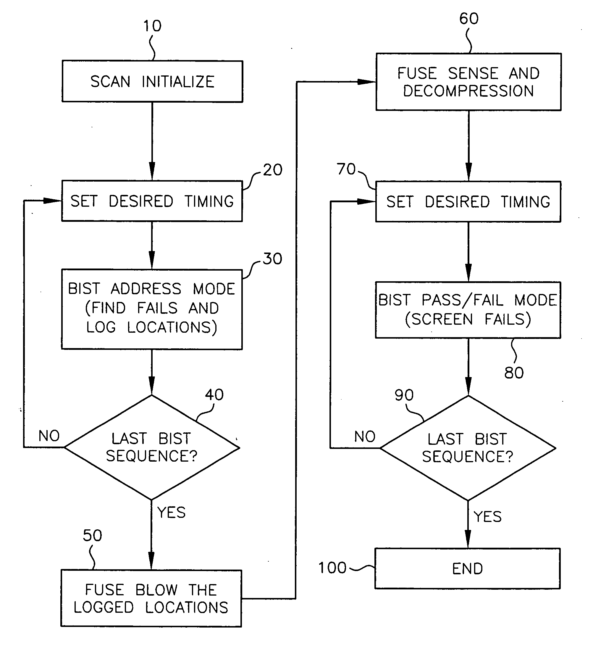
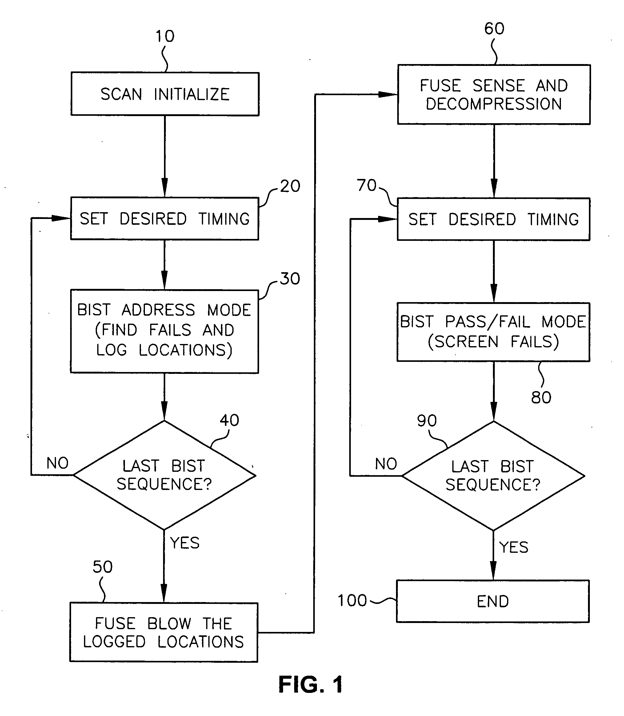
[0028] Most memory arrays, including embedded memory cells such as SRAM cells, have redundancy. That is, the cells have extra cells built into the memory array. If there are faulty cells, the faulty cells can be replaced with redundant cells. The inventors have devised a method of using the built-in self-test to identify weak memory cells, including embedded memory cells such as SRAMs, and to repair them before they are sent to a customer. The repairs are completed by using the built-in redundancy.

[0029] The invention tests the cells at a stress level that is a little harder than the cells would experience in the field under operational conditions run by the customer. Harder testing can be accomplished, for example, by running the cells with a tighter timing than the timing that would be used by the customer under operational conditions. In alternative embodiments, the memory cells may be tested at a higher frequency, or a higher voltage, or a higher temperature, or other harsher e...


PUM


Abstract

A method of manufacturing a device having embedded memory including a plurality of memory cells. During manufacturing test, a first test stress is applied to selected cells of the plurality of memory cells with a built-in self test. At least one weak memory cell is identified. The at least one weak memory cell is repaired. A second test stress is applied to the selected cells and the repaired cells with the built-in self test.

Description

TECHNICAL FIELD [0001] The present invention relates generally to the repair of memory cells used in computer chips and, more particularly, to the repair of embedded memory such as static random access memory (SRAM) cells. BACKGROUND OF THE INVENTION [0002] An application-specific integrated circuit or “ASIC” is an integrated circuit (“IC”) designed to perform a particular function by defining the interconnection of a set of basic circuit building blocks drawn from a library provided by the circuit manufacturer. An ASIC is an IC with functionality customized for a particular use, such as particular equipment or a particular project, rather than being for general-purpose use. For example, a chip designed solely to run a cash register is an ASIC. In contrast, a microprocessor is not application specific because it can be adapted to many purposes. [0003] An “embedded system” is a special-purpose computer system built into a larger device. An embedded system is typically required to mee...

Claims


Application Information

Patent Timeline
Patent Type & Authority Applications(United States)
IPC IPC(8): G01R31/28G11C29/00G11C29/44
CPCG11C11/41G11C29/44G11C2029/0401G11C29/70G11C29/4401
Inventor BRENNAN, CIARAN J.EUSTIS, STEVEN M.FRAGANO, MICHAEL T.OUELLETTE, MICHAEL R.PAI, NEELESH G.ROWLAND, JEREMY P.TOMPSETT, KEVIN M.WAGER, DAVID J.
Owner IBM CORP
Why Eureka
Try Eureka