Silicon-based light emitting diode
a light-emitting diode and silicon-based technology, applied in the field of manufacturing a semiconductor device, can solve the problems of difficult application of silicon-based light-emitting diodes and silicon nano-size dots, and achieve the effects of stable operation, high luminous efficiency, and narrow emission spectrum
- Summary
- Abstract
- Description
- Claims
- Application Information
AI Technical Summary
Benefits of technology
Problems solved by technology
Method used
Image
Examples
first embodiment
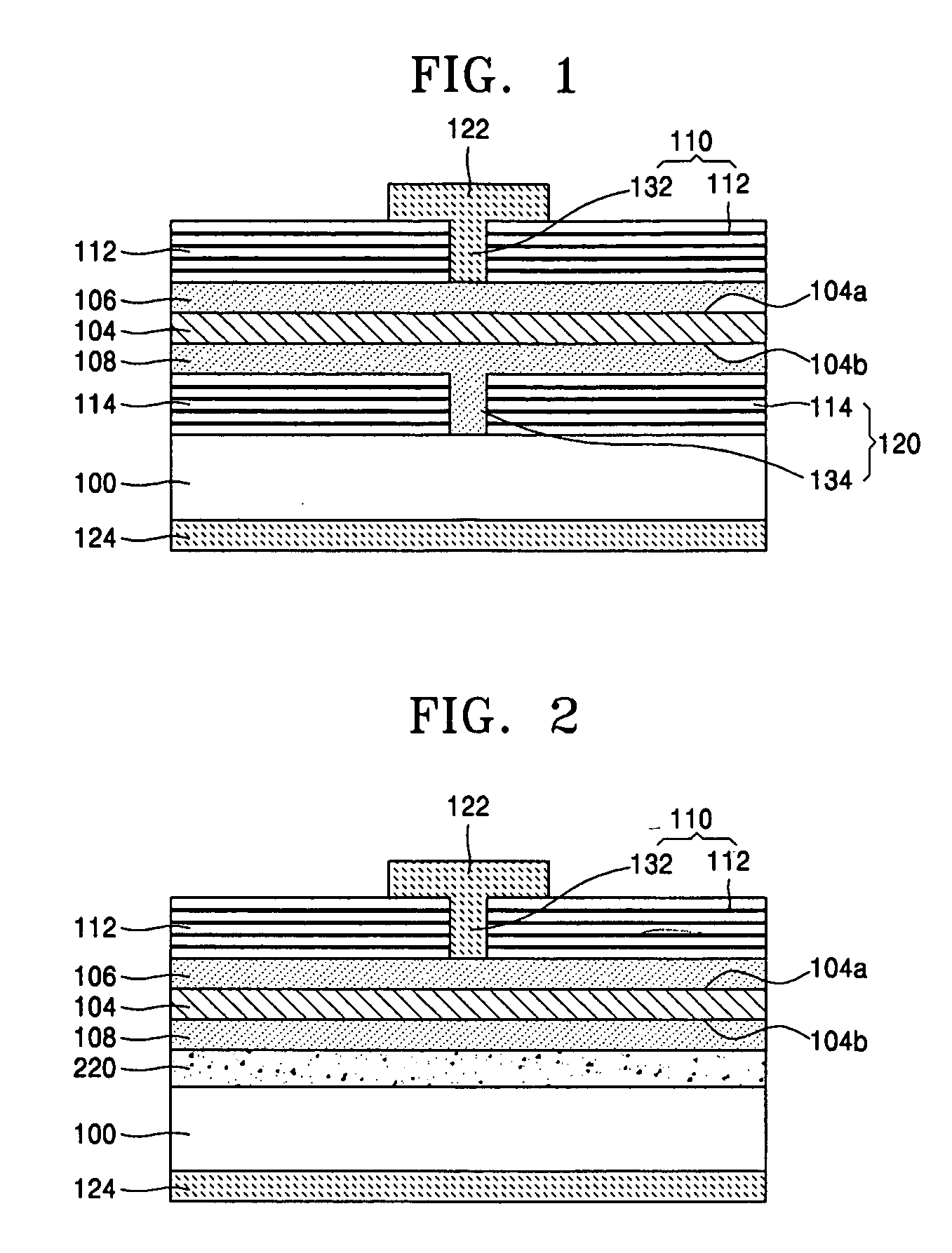
[0020]FIG. 1 is a sectional view showing a major portion of the silicon-based light emitting diode according to the present invention.
[0021] Referring to FIG. 1, the silicon-based light emitting diode according to the first embodiment of the present invention includes an active layer 104 that has a first side 104a and a second side 104b which mutually oppose each other formed on a substrate 100. The active layer 104 is formed of crystalline or amorphous silicon nano-size dots. Preferably, the active layer 104 has a thickness of 150 μm˜30 nm.
[0022] The first side 104a of the active layer 104 faces with a first reflecting portion 110. Also, the second side 104b of the active layer 104 faces with a second reflecting portion 120.
[0023] A first doping layer 106 is interposed between the active layer 104 and the first reflecting portion 110. Also, a second doping layer 108 is interposed between the active layer 104 and the second reflecting portion 120.
[0024] A first electrode 122 is f...
second embodiment
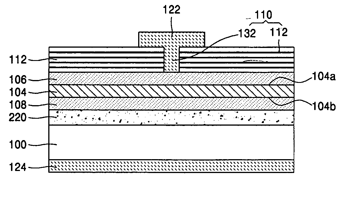
[0028]FIG. 2 is a sectional view showing a major portion of the silicon-based light emitting diode according to the present invention.
[0029] The second embodiment is mostly similar to the first embodiment, which is however different from the first embodiment in that a second reflecting portion 220 is formed of a total internal reflection metal layer. In other words, the first reflecting portion 110 includes the DBR 112 obtained by alternately stacking two kinds of silicon-containing insulating layers with different compositions and the gate 132 formed by penetrating through the DBR 112. Then, the second reflecting portion 220 is formed of the total internal reflecting metal layer. In FIG. 2, like reference numerals of the first embodiment designate the same parts with no specific description.
[0030] Referring to FIG. 2, upon applying current to the first electrode 122 and the second electrode 124, the carriers consisting of electrons or holes reach the first doping layer 106 through...
PUM
 Abstract
Description
Claims
Application Information

