Image sensor package and method for manufacturing the same

a technology of image sensor and package, which is applied in the direction of color television, solid-state devices, television systems, etc., can solve the problem of restricting the adjustment of focal distance, and achieve the effect of reducing the structure height of the image sensor package, and reducing the structure heigh

Inactive Publication Date: 2005-06-30
ADVANCED SEMICON ENG INC
View PDF6 Cites 36 Cited by
  • Summary
  • Abstract
  • Description
  • Claims
  • Application Information

AI Technical Summary

Benefits of technology

[0012] According to the structure of the image sensor package in the invention, the chip is coupled to the substrate by a flip-chip type, so that the structure height of the image sensor package can be reduced. Moreover, the transparent cover directly cove

Problems solved by technology

Since the total height, which is a distance between the lens and the sub

Method used


Image

  • Image sensor package and method for manufacturing the same
  • Image sensor package and method for manufacturing the same
  • Image sensor package and method for manufacturing the same

Examples


Embodiment Construction

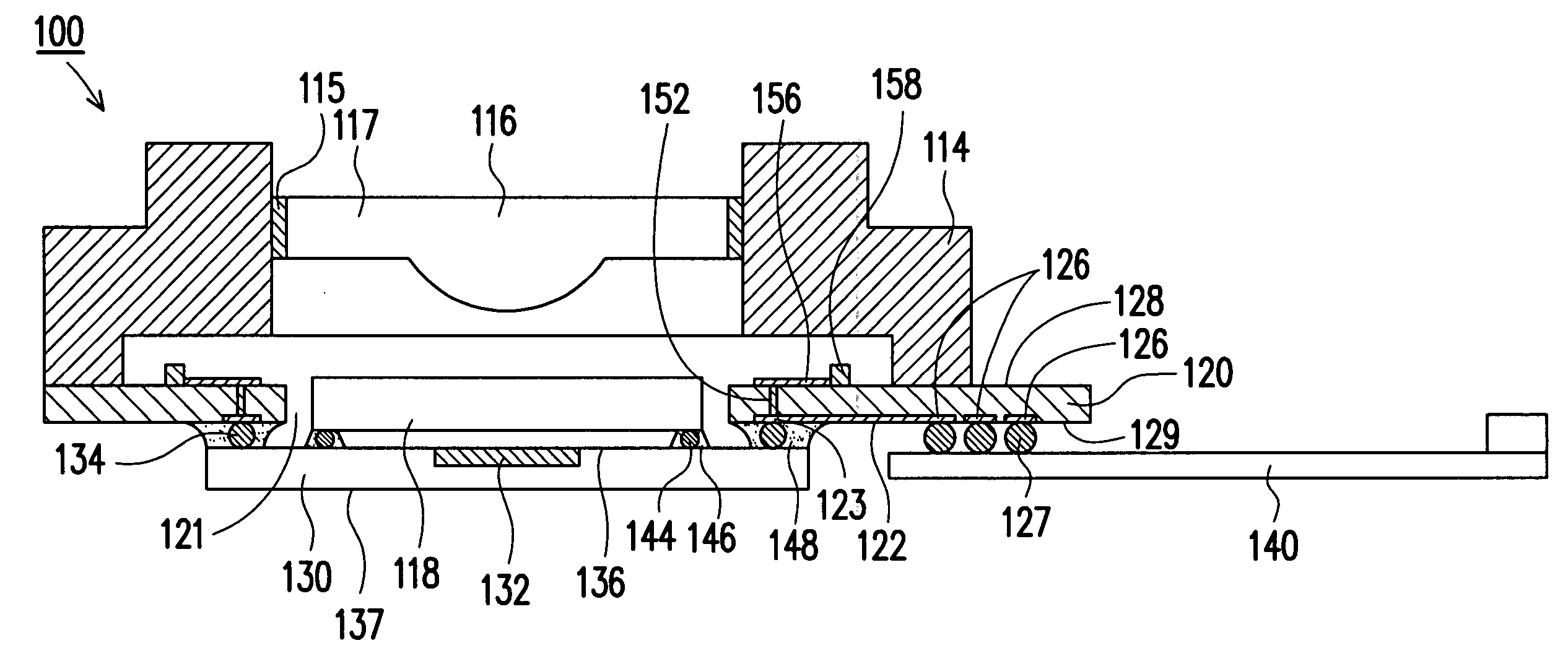
[0018] Referring to FIG. 3, it is a cross-sectional view, schematically illustrating a structure of an image sensor package 100, according to embodiment of the invention. The structure of an image sensor package 100 includes a chip 130, a transparent cover 118, a substrate 120, and a lens module 116. The chip 130 has an active surface 136, a back surface 137, an optical sensing device 132, and multiple bumps 134 disposed on the active surface 136. The bumps 134 are located at the peripheral region of the active surface on the chip 130. In detail, the bumps 134 can be disposed on one side, two sides, three sides, or four sides of the active surface 136. The optical sensing device 132 can be a Complementary Metal-Oxide Semiconductor (CMOS) device or a charge coupled device (CCD). The bumps 134 can be a gold bump or a solder bump.

[0019] The transparent cover 118 is adhered to the chip 130 by a sealant 146 and covers the optical sensing device 132. The sealant 146 can be an UV adhesive...


PUM


Abstract

An image sensor package includes a substrate, a chip, a transparent cover, and a lens module. The substrate has an upper surface and a lower surface, and has a plurality of connection pads disposed on the lower surface and a though opening. The chip has an active surface, and has an image sensor disposed on the active surface, corresponding to the through opening of the substrate. Also and, a plurality of bumps are disposed at peripheral region of the active surface and are electrically connected to the pads. The transparent cover is disposed in the through opening of the substrate and covers the image sensor. The lens module is disposed on the upper surface for transmitting light to the image sensor.

Description

CROSS-REFERENCE TO RELATED APPLICATION [0001] This application claims the priority benefit of Taiwan application serial no. 92137701, filed on Dec. 31, 2003. BACKGROUND OF THE INVENTION [0002] 1. Field of Invention [0003] The present invention relates to structure of image sensor package. More particularly, the present invention relates to structure of image sensor package having a reduced height in whole structure. [0004] 2. Description of Related Art [0005] The image sensor semiconductor is a semiconductor chip, in which the optical signals are converted into electric signals. The image sensor semiconductor includes an optical sensing device, such as a complementary metal-oxide semiconductor (CMOS) device or a charge coupled device (CCD). [0006] Taking the U.S. Pat. No. 5,636,104 as a reference of the invention, it discloses a structure of image sensor package 10, as shown in FIG. 1. The structure of image sensor package 10 includes a chip 30, a housing 14, a lens 16, a glass 18, ...

Claims


Application Information

Patent Timeline
IPC IPC(8): H01L27/14H01L31/0203H01L31/0232H04N5/335H04N5/372H04N5/374
CPCH01L27/14618H01L27/14625H01L27/14687H01L31/0203H01L31/0232H01L2224/32013H01L2224/48091H01L2224/48227H01L2924/15311H01L2224/32225H01L2924/00014H01L31/02325
Inventor YEE, KUO-CHUNG
Owner ADVANCED SEMICON ENG INC
Why Eureka
Try Eureka