Method of embedding semiconductor element in carrier and embedded structure thereof

a semiconductor element and carrier technology, applied in semiconductor devices, semiconductor/solid-state device details, electrical devices, etc., can solve the problems of cubga packages, substrates b>31/b> must be turned over twice, and the size or height of packages is difficult to reduce, so as to simplify the semiconductor packaging process, reduce the overall thickness or size of fabricated semiconductor devices, and easy to remov

Active Publication Date: 2006-04-25
PHOENIX PRECISION TECH CORP
View PDF9 Cites 11 Cited by
  • Summary
  • Abstract
  • Description
  • Claims
  • Application Information

AI Technical Summary

Benefits of technology

[0014]A primary objective of the present invention is to provide a method of embedding a semiconductor element in a carrier and an embedded structure thereof, so as to effectively position the semiconductor element in the carrier.
[0015]Another objective of the invention is to provide a method of embedding a semiconductor element in a carrier and an embedded structure thereof, in which when the semiconductor element is placed in a hole of the carrier, a medium material is applied prior to glue in the hole to allow easy removal of an auxiliary material from the carrier.
[0017]A further objective of the invention is to provide a method of embedding a semiconductor element in a carrier and an embedded structure thereof, which can prevent the problems encountered in fabricating semiconductor packages in the prior art.
[0018]A further objective of the invention is to provide a method of embedding a semiconductor element in a carrier and an embedded structure thereof, which can reduce the overall height of the structure.
[0019]A further objective of the invention is to provide a method of embedding a semiconductor element in a carrier and an embedded structure thereof, so as to integrate a semiconductor chip and a chip carrier, thereby providing better flexibility in structure design for a client, and simplifying the fabrication processes, reducing the cost and solving the interface integration problem.
[0023]In the present invention, a medium material is applied prior to glue to separate an auxiliary material from the glue such that the auxiliary material can be easily removed without being bound to the glue. Moreover, the semiconductor element can be firmly positioned in a hole of the carrier via the glue, thereby prevent the semiconductor element from dislocation in subsequent fabrication processes. Furthermore, by the present invention the semiconductor element can be embedded and received in the hole of the carrier, making the overall thickness or size of a fabricated semiconductor device desirably reduced as well as simplifying the semiconductor packaging processes. This thereby provides better flexibility in structure for a client, simplifies the fabrication processes for semiconductor manufacturers, and solves the interface integration problem of the semiconductor package.

Problems solved by technology

This vertical stacking or mounting manner increases the overall height of the BGA package, making it hard to reduce the size or height of the package.
Compared to the CDBGA package, one drawback of the CUBGA package is that the substrate 31 must be turned over twice to complete the electrical connection.
However, since the chip 22, 32 is positioned and held in place by means of the tape 26, 36 and the encapsulation body 24, 34, the package cannot be subject to other connection manners such as stacking of multiple chips or stacking of multiple substrates, thereby reducing the flexibility in application of the packaged product.
As a result, the appearance of the package is deteriorated.
Furthermore, for a wire-bonded package or a flip-chip package that is employed frequently for the chip package now, the substrate fabricating process and the chip packaging process require different machines and procedures, making the fabrication processes of the package very complicated and costly.
In particular for the wire-bonded package, the bonding wires are arranged in very high density around the chip, which would easily lead to contact between adjacent wires and cause short circuit, thereby increasing the difficulty in performing the wire-bonding process.
However, in practice, due to the various designs of semiconductor packages, the size of the mold cavity and clamping positions do not always match any particular semiconductor structure to be packaged, which may cause a problem of insufficient clamping and in such a case, the epoxy material would easily flash to the surface of the substrate.
This not only affects the planarity and appearance of the semiconductor package, but may also contaminate the area on the substrate where the solder balls are to be implanted.
As a result, the quality of electrical connection as well as the yield and reliability of the semiconductor package are seriously degraded.
Therefore, the fabrication processes of the semiconductor device involve a number of different manufacturers, including the chip carrier manufacturer and the semiconductor packaging manufacturer, thereby making the fabrication processes complicated in practice and not easy to achieve interface integration.
In case the client wishes to modify the product design, the changes and integration involved are even more complicated, not meeting the requirements of flexibility in change and economical benefit.

Method used


Image

  • Method of embedding semiconductor element in carrier and embedded structure thereof
  • Method of embedding semiconductor element in carrier and embedded structure thereof
  • Method of embedding semiconductor element in carrier and embedded structure thereof

Examples


first preferred embodiment

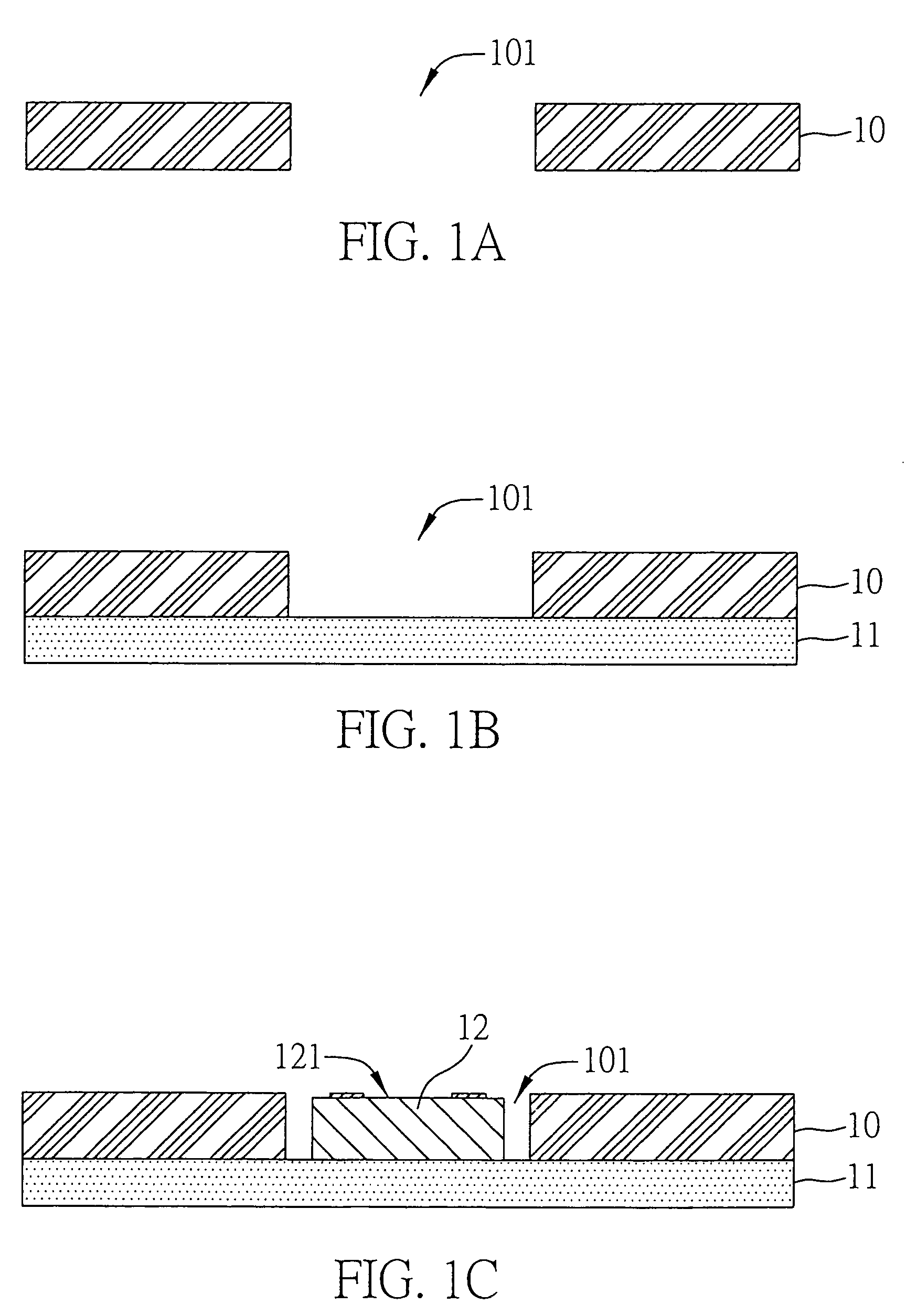
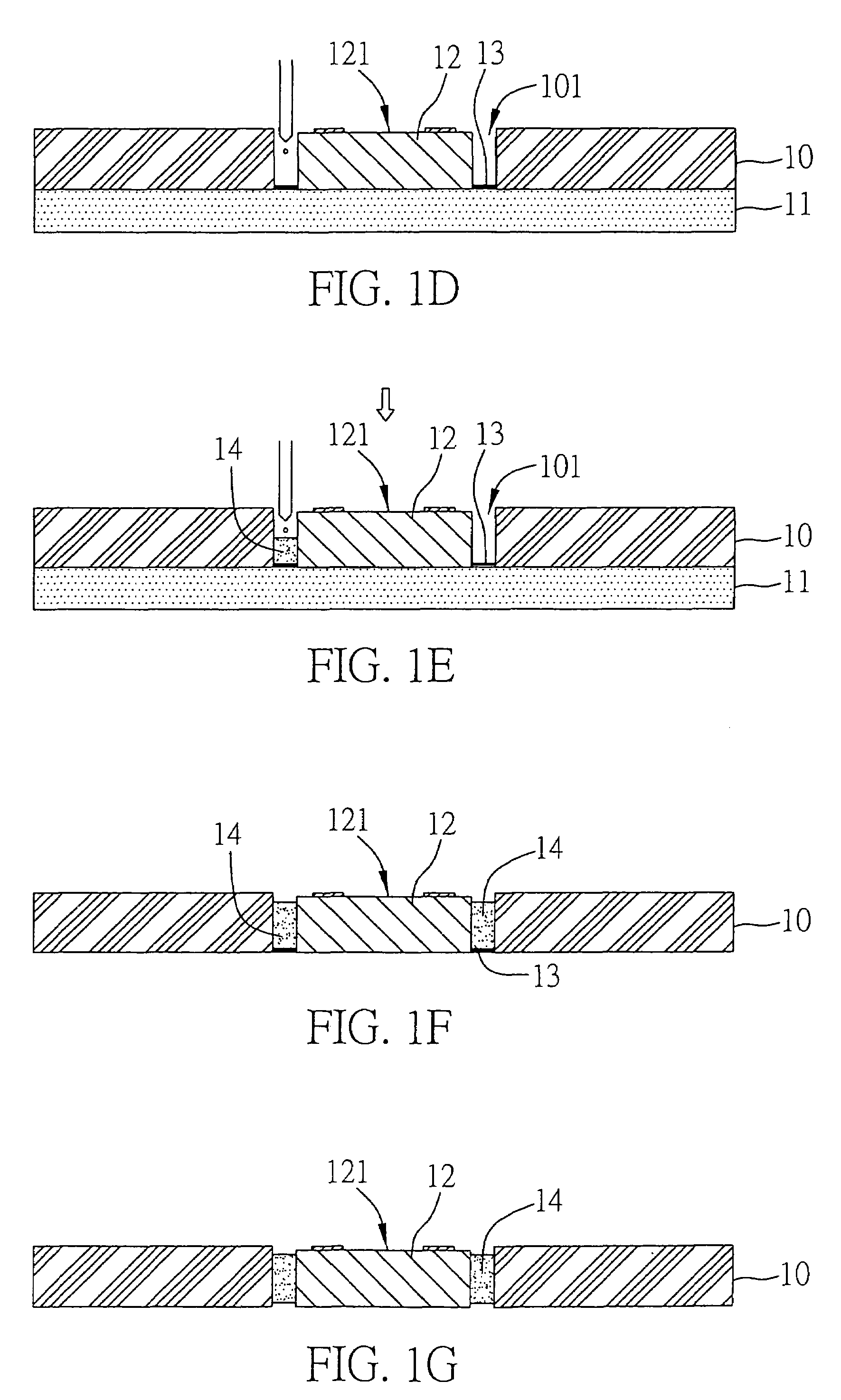
[0032]FIGS. 1A to 1G show procedural steps of a method of embedding a semiconductor element in a carrier in accordance with a first preferred embodiment of the present invention.

[0033]Referring to FIG. 1A, first, a carrier 10 is prepared, which can be an insulating board, metal board, or circuit board having a circuit layer. At least one hole 101 is formed through the carrier 10.

[0034]Referring to FIG. 1B, an auxiliary material 11 is attached to the bottom of the carrier 10 and temporarily seals a bottom opening of the hole 101 of the carrier 10. The auxiliary material 11 can be made as a film, dry film, insulating board or metal board, and a surface of the auxiliary material 11 in contact with the carrier 10 can be made adhesive or slightly adhesive.

[0035]Referring to FIG. 1C, a semiconductor element 12 such as semiconductor chip is placed in the hole 101 of the carrier 10 in a manner that an active surface 121 of the semiconductor element 12 is exposed from the hole 101 and the se...

second preferred embodiment

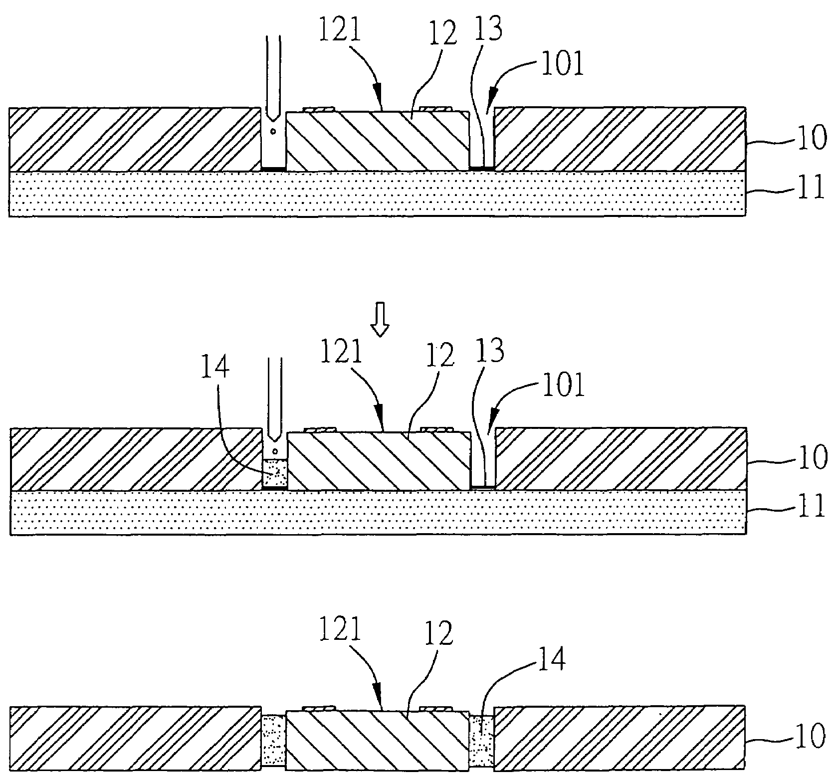
[0041]FIGS. 2A to 2G show procedural steps of the method of embedding a semiconductor element in a carrier in accordance with a second preferred embodiment of the present invention. In this embodiment, an auxiliary material used is the same as that of the first embodiment with its surface being made adhesive, slightly adhesive or non-adhesive.

[0042]Referring to FIGS. 2A and 2B, first, a carrier 10 having a hole 101 is provided. A slightly adhesive auxiliary material 11 is attached to the bottom surface of the carrier 10 and temporarily seals a bottom opening of the hole 101 of the carrier 10.

[0043]Referring to FIG. 2C, a medium material 13 is applied in the hole 101 to form a layer of medium material 13 at the bottom of the hole 101.

[0044]Referring to FIG. 2D, then a semiconductor element 12 is place in the hole 101 in a manner that an active surface 121 of the semiconductor element 12 is exposed from the hole 101. Since the medium material 13 when in a liquid phase before being cur...


PUM


Abstract

A method of embedding a semiconductor element in a carrier and an embedded structure thereof are proposed. First, a carrier having a hole is provided and an auxiliary material is attached to a side of the carrier. A semiconductor element is placed in the hole of the carrier. Then, a medium material and glue are applied in order in the hole to firmly position the semiconductor element in the hole of the carrier via the glue. Finally, the auxiliary material and the medium material are removed to form a structure with the semiconductor element being embedded in the carrier, thereby eliminating the drawbacks encountered in packing the semiconductor element in the prior art.

Description

FIELD OF THE INVENTION[0001]The present invention relates to method of embedding semiconductor elements in carriers and embedded structures thereof, and more particularly, to a method of embedding a semiconductor chip in a hole of a carrier and a chip embedded structure.BACKGROUND OF THE INVENTION[0002]As the semiconductor packaging technology advances, there have been developed many different types of semiconductor packages. In general, a semiconductor package is formed by mounting a semiconductor chip on a substrate or lead frame, electrically connecting the chip to the substrate or lead frame, and then encapsulating the chip and the substrate or lead frame via a resin material. One of the advanced semiconductor packages is referred to as ball grid array (BGA) package, which is characterized in using a circuit board with the chip being mounted on a front surface thereof, and implanting a plurality of array-arranged solder balls on a back surface of the circuit board via a self-ali...

Claims


Application Information

Patent Timeline
Patent Type & Authority Patents(United States)
IPC IPC(8): H01L21/50H01L21/56H01L21/58H01L21/68H01L23/02H01L23/13H01L23/31H01L23/538
CPCH01L21/568H01L23/3128H01L24/83H01L24/96H01L24/29H01L23/13H01L2924/014H01L23/5389H01L2224/48091H01L2224/8385H01L2924/01005H01L2924/01082H01L2924/07802H01L2924/15311H01L2924/1532H01L2924/18162H01L2224/48227H01L2924/0665H01L24/48H01L2224/2919H01L2924/01006H01L2924/01033H01L2924/00014H01L2924/00H01L2924/181H01L2924/18165H01L2924/00012H01L2224/45099H01L2224/45015H01L2924/207
Inventor CHEN, CHI-MING
Owner PHOENIX PRECISION TECH CORP
Why Eureka
Try Eureka