Semiconductor device and manufacturing method therefor

Inactive Publication Date: 2005-06-30
LAPIS SEMICON CO LTD
View PDF2 Cites 2 Cited by
  • Summary
  • Abstract
  • Description
  • Claims
  • Application Information

AI Technical Summary

Benefits of technology

[0008] The present invention makes it possible to fabricate a semiconductor device that permits free setting of characteristics of individual semiconductor elements which have different characteristics and are mixedly mounted, and is free of a step between deposited semiconductor elements. It is possible therefore t

Problems solved by technology

However, according to the semiconductor devices disclosed in Patent Documents 1 and 2, large steps are produced between portions wherein semiconductor elements having different characteristics are formed, making it difficult to achieve microminiaturization from the aspects of uniformity of resists, control of contact depths, processability of wires, etc.
Such partial epita

Method used


Image

  • Semiconductor device and manufacturing method therefor
  • Semiconductor device and manufacturing method therefor
  • Semiconductor device and manufacturing method therefor

Examples


first embodiment

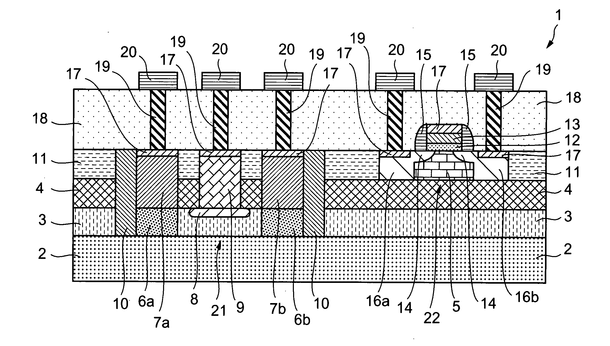
[0022]FIG. 1 is a sectional view schematically showing a configuration of an essential section of a semiconductor device 1 of a first embodiment according to the present invention.

[0023] As shown in FIG. 1, the semiconductor device 1 includes a junction transistor 21 serving as a first semiconductor element deposited on an n− silicon layer 3, which is a second semiconductor layer epitaxially grown on a p-type silicon substrate 2, which is a first semiconductor layer, and a MOS transistor 22 serving as a second semiconductor element deposited on a silicon-on-insulator (SOI) layer 5, which is a third semiconductor layer existing through the intermediary of a buried oxide (BOX) layer 4 serving as an insulating layer on the n-silicon layer 3.

[0024] Deposited in the region wherein the junction transistor 21 is formed are a source (drain) layer 6a and a drain (source) layer 6b of the junction transistor 21 that are made of n+ silicon, buried layers 7a, 7b made of n+ polysilicon, a gate ...

second embodiment

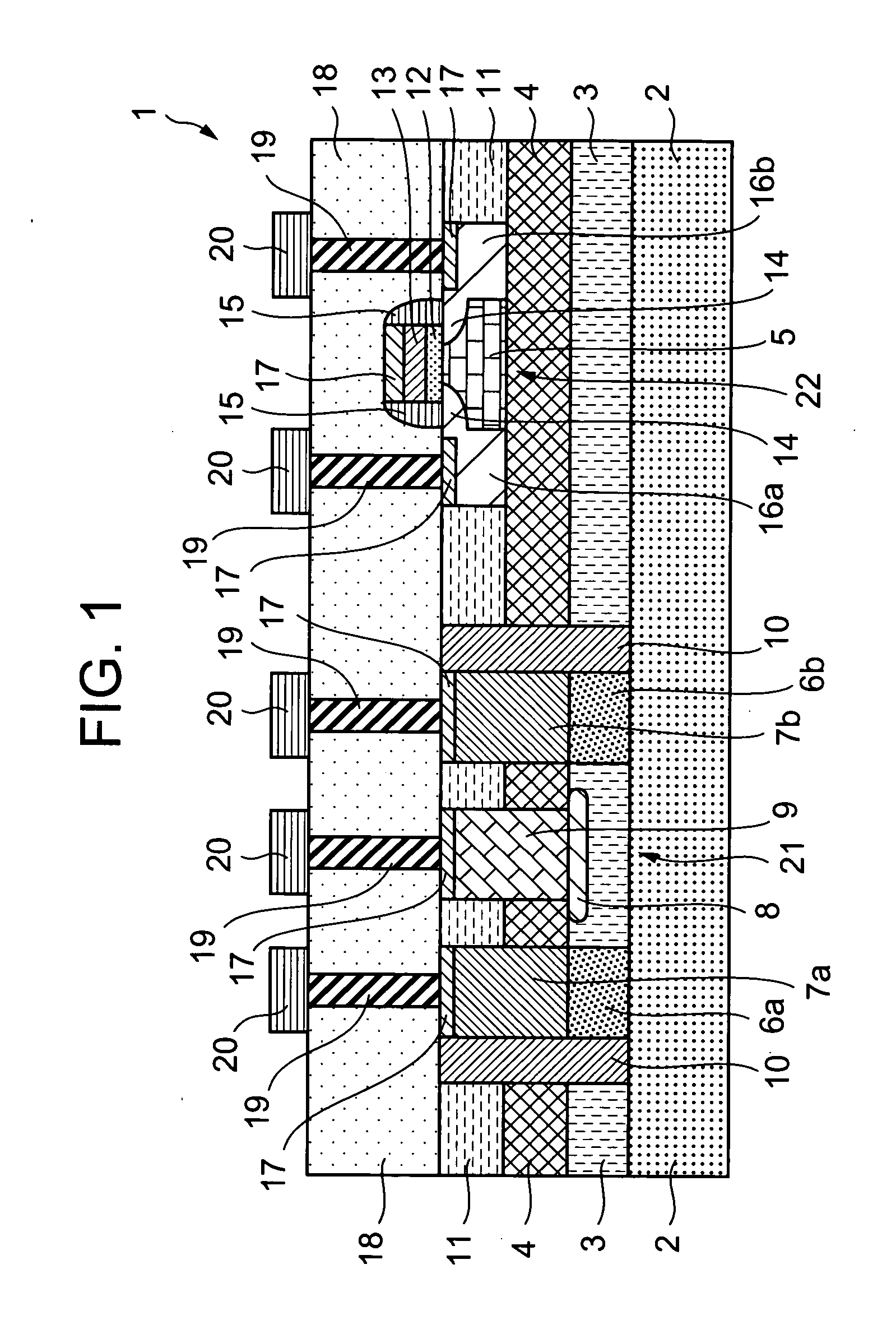
[0040]FIG. 9 is a sectional view schematically showing the configuration of an essential section of a semiconductor device 31 of a second embodiment according to the present invention. In the semiconductor device 31, the same component elements as those of the semiconductor device 1 of the first embodiment shown in FIG. 1 will be assigned the same reference numerals.

[0041] As shown in the figure, the semiconductor device 31 includes a MOS high voltage transistor 41 serving as a first semiconductor element deposited on a p− silicon layer 33, which is a second semiconductor layer epitaxially grown on an n-type silicon substrate 32, which is a first semiconductor layer, and a MOS transistor 22 serving as a second semiconductor element deposited on an SOI layer 5, which is a third semiconductor layer existing through the intermediary of a BOX layer 4 serving as an insulating layer on the p− silicon layer 33.

[0042] Formed in the region wherein the MOS high voltage transistor 41 is form...


PUM


Abstract

The present invention provides a semiconductor device that permits free setting of characteristics of individual semiconductor elements which are mixedly mounted and have different characteristics, and is free of steps between formed semiconductor elements, and a manufacturing method for the same. In the semiconductor device, an n-type silicon layer is deposited on a p-type silicon substrate by epitaxial growth, and then an SOI layer is deposited thereon through the intermediary of a BOX layer. A junction transistor using a part of the n-type silicon layer as a channel region and a MOS transistor using the SOI layer are produced. The semiconductor device ensures uniform resist, control of contact depths, wire processability, etc., making the semiconductor device ideally suited for microminiaturization.

Description

BACKGROUND OF THE INVENTION [0001] 1. Field of the Invention [0002] The present invention relates to a semiconductor device and a manufacturing method therefor and, more particularly, to a semiconductor device having semiconductor elements with different characteristics mixedly incorporating and a manufacturing method therefor. Description of the Related Art Hitherto, as this type of semiconductor devices, there has been one, for example, in which an SOI layer is partly removed, and then a bulk device is deposited on an exposed Si substrate (refer to, for example, Patent Document 1, Japanese Unexamined Patent Application Publication No. H1-183145). There has been another one in which the surface of each semiconductor layer of a plurality of semiconductor layers provided through the intermediary of insulating films is exposed, and then an impurity is implanted through the exposed surface and diffused to form each semiconductor element (refer to, for example, Patent Document 2, Japane...

Claims


Application Information

Patent Timeline
IPC IPC(8): H01L21/02H01L21/28H01L21/337H01L21/76H01L21/762H01L21/768H01L21/8232H01L21/8234H01L21/84H01L27/06H01L27/08H01L27/088H01L27/12H01L29/417H01L29/423H01L29/49H01L29/786H01L29/808
CPCH01L27/1203H01L21/84
Inventor TANAKA, HIROYUKI
Owner LAPIS SEMICON CO LTD
Why Eureka
Try Eureka