Liquid crystal display device and inspection method for a transparent substrate
a technology of liquid crystal display and inspection method, which is applied in the direction of optics, optical radiation measurement, instruments, etc., can solve the problems of difficult improvement of yield, and achieve the effect of confirming easily uneven thickness of transparent substrate, good dark appearance, and confirming easily uneven thickness
- Summary
- Abstract
- Description
- Claims
- Application Information
AI Technical Summary
Benefits of technology
Problems solved by technology
Method used
Image
Examples
example 1
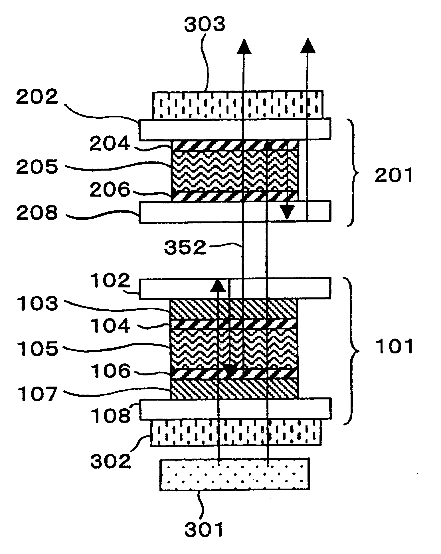
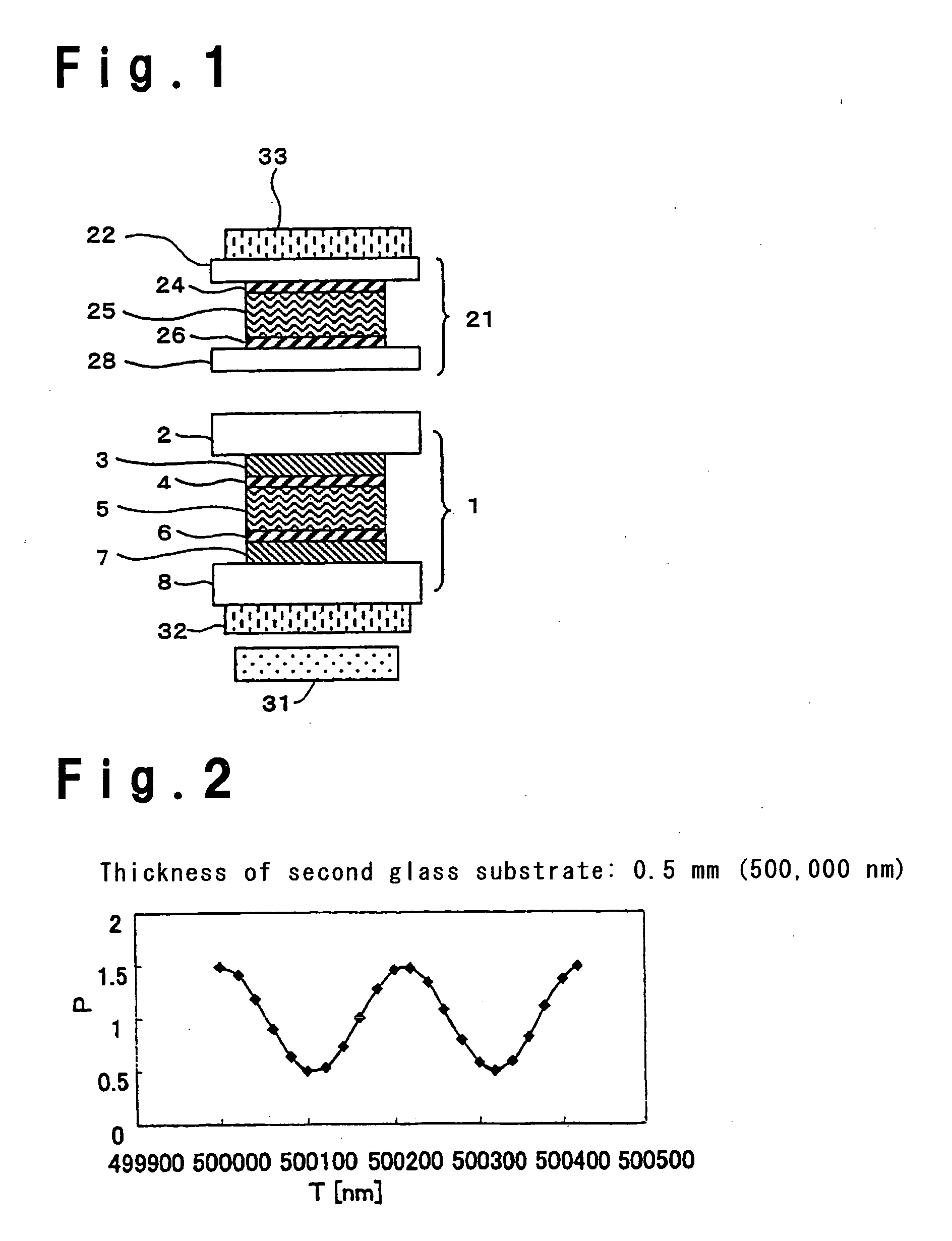
[0131] A displaying cell was prepared in a manner as follows. A transparent electrode is disposed on each of two glass substrates of 0.7 mm thick, and an alignment film was formed on each of the transparent electrodes. A rubbing treatment was conducted to alignment films. In the rubbing treatment, the direction of rubbing was determined so as to form a twist angle of 180° in a state that the two glass substrates were combined by interposing liquid crystal therebetween. After the rubbing, the glass substrates were piled up so that the transparent electrodes each having the alignment film oppose to each other and liquid crystal was injected between the glass substrates in a shield state. As the liquid crystal, a commercially available liquid crystal (“ZLI4431”: Δn=0.1643 manufactured by Merck) was used. The cell gap was 6 μm and Δn·d was 0.986 μm.
[0132] A compensation cell was prepared in a manner as follows. An alignment film was formed on each of two glass substrates of 0.55 mm thi...
example 2
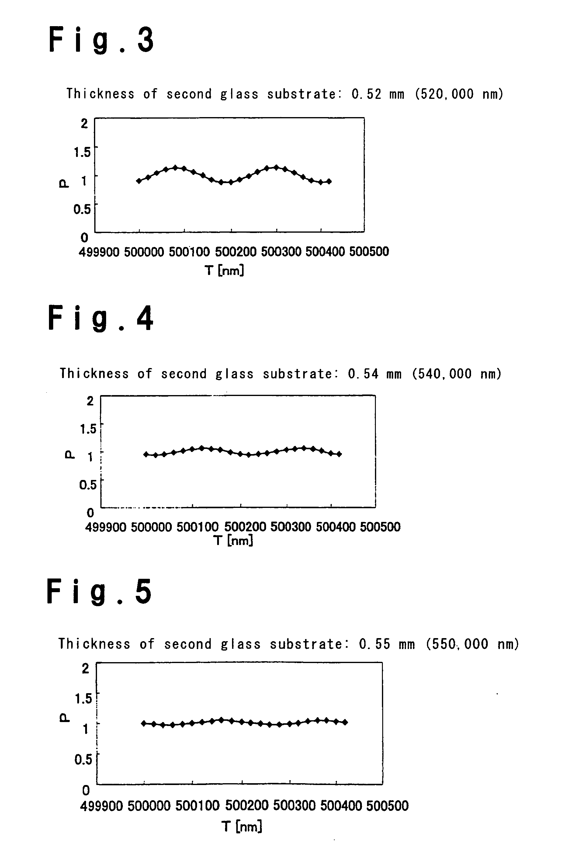
[0137] Glass substrates of 0.55 mm thick were used for the glass substrates of the displaying cell, and glass substrates of 0.5 mm thick were used as the glass substrates of the compensation cell. Then, a liquid crystal display device was prepared in the same manner as Example 1. The difference of thickness between adjacent glass substrates in the displaying cell and the compensation cell is 0.05 mm. A display of good dark appearance was obtained without generating a line-shaped ununiformity of brightness in a case that no voltage was applied to the liquid crystal layer of the displaying cell.
example 3
[0138] A glass substrate of 0.55 mm thick was used as the glass substrate at a front surface side of the displaying cell, and a glass substrate of 0.5 mm thick was used as the glass substrate at a rear surface side of the displaying cell. Further, glass substrates of 0.5 mm thick were used for the glass substrates of the compensation cell. Then, a liquid crystal display device was prepared in the same manner as Example 1. The difference of thickness between adjacent glass substrates in the displaying cell and the compensation cell is 0.05 mm. A display of good dark appearance could be obtained without generating a line-shaped ununiformity of brightness in a case that no voltage was applied to the liquid crystal layer of the displaying cell.
[0139] A liquid crystal display device was prepared in the same manner as Comparative Example 1 except that glass substrates of 0.55 mm thick were used for the glass substrates of the displaying cell and the glass substrates of the compensation c...
PUM
| Property | Measurement | Unit |
|---|---|---|
| thickness | aaaaa | aaaaa |
| angle | aaaaa | aaaaa |
| thickness | aaaaa | aaaaa |
Abstract
Description
Claims
Application Information


