Liquid crystal display and fabricating method thereof

a technology of liquid crystal display and fabrication method, which is applied in the direction of optics, instruments, electrical equipment, etc., can solve the problems of difficult to obtain stable picture, poor comparison ratio of liquid crystal display device of type n, and inability to achieve stable picture quality, etc., to achieve the effect of increasing the viewing angl

Active Publication Date: 2005-06-30
LG DISPLAY CO LTD
View PDF6 Cites 58 Cited by
  • Summary
  • Abstract
  • Description
  • Claims
  • Application Information

AI Technical Summary

Benefits of technology

[0012] An object of the present invention is to provide a liquid crystal display device implemented with the rib to increase the viewing angle, and method of fabricating the same.

Problems solved by technology

However, the TN type liquid crystal display device has a poor comparison ratio because light is not completely shut off at an off state.
In addition, the comparison ratio changes with angles, and the brightness of middle scale reverses with change in the comparison ratio, thus, it is difficult to obtain a stable picture.
Furthermore, the poor comparison ratio causes a viewing-angle problem such that the picture quality is not symmetric to the front surface.
In addition, when the voltage is applied between the pixel electrode and a common electrode formed on an upper substrate, an electric field distortion is generated by the rib.
However, the liquid crystal display of the related art requires the rib formed by a separate mask process and complicates the production process of the liquid crystal display device.

Method used


Image

  • Liquid crystal display and fabricating method thereof
  • Liquid crystal display and fabricating method thereof
  • Liquid crystal display and fabricating method thereof

Examples


first embodiment

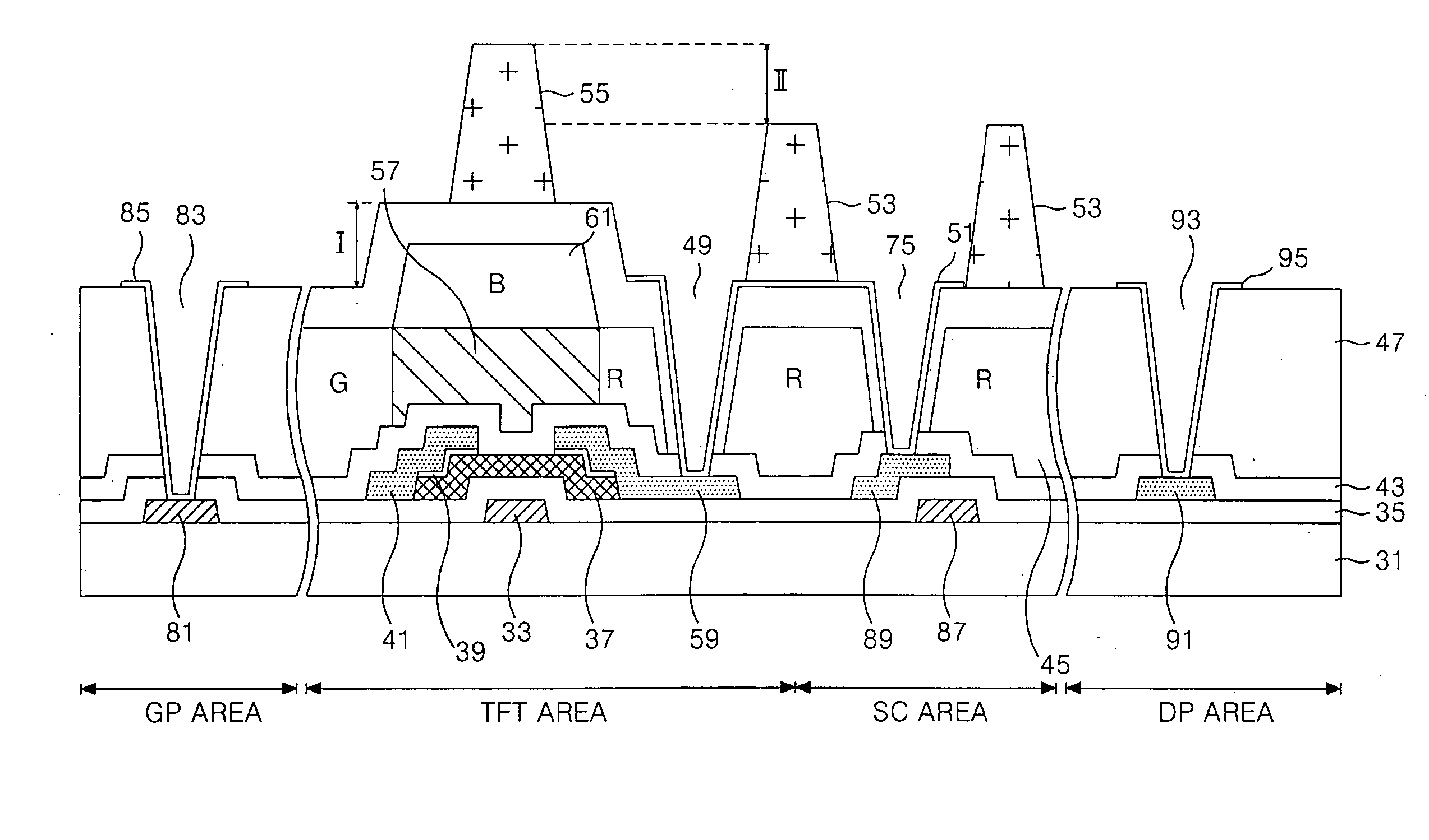
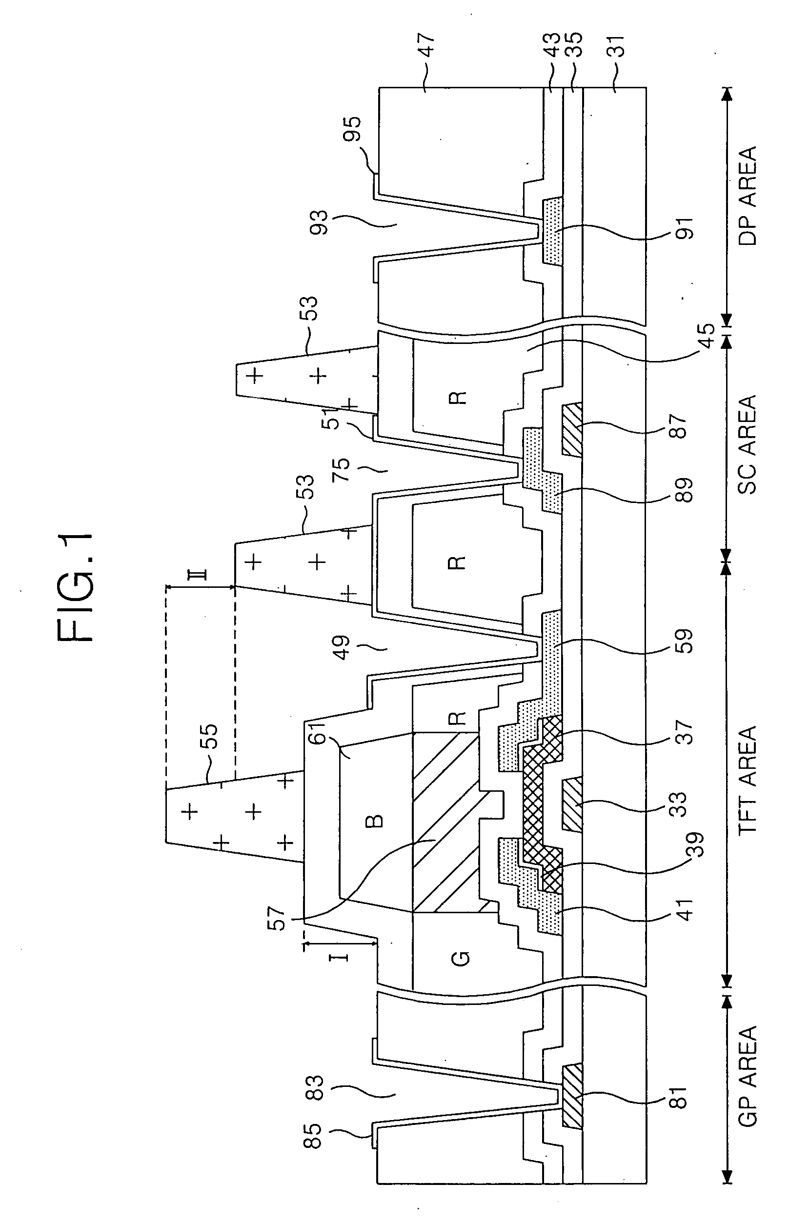
[0029]FIG. 1 is a cross-sectional view of a liquid crystal display device according to the present invention.

[0030] A liquid crystal display, as shown in FIG. 1, includes a thin film transistor TFT formed at an intersection of a gate line 87 and a data line, a pixel electrode 51 connected to the thin film transistor, a storage capacitor SC formed at an overlapping area of the gate line 87 and a storage electrode 89, a gate pad connected to the gate line 87, a data pad DP connected to the data line, a spacer 55 to sustain a cell gap, and a rib 53 having the same height as the spacer 55.

[0031] The thin film transistor responds to a gate signal from the gate line 87 to charge the pixel electrode 51 with a pixel signal provided from the data line and maintains the preceding pixel signal. To achieve this, the thin film transistor includes a gate electrode 33 connected to the gate line 87, a source electrode 41 connected to the data line, and a drain electrode 59 connected to the pixel e...

second embodiment

[0057] Thereafter, as shown in FIG. 4C, the spacer 55 and the rib 53 are formed on the pixel electrode 51 and the color filter 45 of the thin film transistor, thereby completing the liquid crystal display according to the present invention.

[0058] According to the above-described composition, the difference in height of the stepped differences I and II is influenced by the presence of the light shielding layer 57 and the dummy color filter 61. The stepped difference II of the spacer 55 and the rib 53 can be increased in accordance with the structure of the instant liquid crystal display device to prevent the occurrence of the alignment defect and the light leakage.

[0059]FIG. 5 is a cross-sectional view representing a thin film transistor array substrate according to a third exemplary embodiment of the present invention.

[0060] Referring to FIG. 5, the thin film transistor array substrate according to the third exemplary embodiment of the present invention prevents the generation of ...


PUM

PropertyMeasurementUnit
electrical resistivityaaaaaaaaaa
thicknessaaaaaaaaaa
thicknessaaaaaaaaaa

Abstract

A liquid crystal display includes a gate line disposed on a substrate; a data line disposed on the substrate, a pixel area being defined by an intersection of the gate line and the data line; a thin film transistor locating at the intersection of the gate line and the data line; a color filter disposed at each pixel area on the substrate; a spacer formed on a first base surface of the thin film transistor area; a rib formed on a second base surface of the pixel area; and a dummy pattern disposed at the thin film transistor area to form a stepped difference of the first base surface and the second base surface.

Description

[0001] This application claims the benefit of Korean Patent Application No. 2003-0099811 filed in Korea on Dec. 30, 2003, which is hereby incorporated by reference. BACKGROUND OF THE INVENTION [0002] 1. Field of the Invention [0003] The present invention relates to a liquid crystal display, and more particularly, to a liquid crystal display for realizing an increased viewing angle by dividing the arrangement direction of liquid crystal material in a pixel area, and a fabricating method thereof. [0004] 2. Discussion of the Related Art [0005] Liquid crystal display (LCD) devices have many advantageous characteristics including low voltage drive, low power consumption, short response time, small size, light weight, small thickness, full color image display and others characteristics. Thus, application of the LCD devices in various types of consumer electronics, from a watch, a calculator, a PC monitor, a notebook, a PDA, an aeronautical monitor, a TV, a mobile phone and other electroni...

Claims


Application Information

Patent Timeline
Patent Type & Authority Applications(United States)
IPC IPC(8): G02F1/136G02F1/1333G02F1/1335G02F1/1339G02F1/1343G02F1/1362G02F1/139H01L21/027H01L29/786
CPCG02F1/133707G02F2001/136222G02F1/1393G02F1/13394G02F1/136222G02F1/136
Inventor KIM, WOONG-KWONPARK, SEUNG-RYUL
Owner LG DISPLAY CO LTD
Why Eureka
Try Eureka