

Method of packaging an optical sensor
a technology of optical sensors and packaging, applied in the field of image and optical sensors, can solve the problems of large package form factor, low optical quality, and high cost of qfp, and achieve the effect of avoiding residue on the lens and avoiding potential surface scratches
- Summary
- Abstract
- Description
- Claims
- Application Information
AI Technical Summary
Benefits of technology
Problems solved by technology
Method used
Image

Examples
Embodiment Construction
[0016] The detailed description set forth below in connection with the appended drawings is intended as a description of the presently preferred embodiments of the invention, and is not intended to represent the only forms in which the present invention may be practiced. It is to be understood that the same or equivalent functions may be accomplished by different embodiments that are intended to be encompassed within the spirit and scope of the invention.
[0017] Certain features in the drawings have been enlarged for ease of illustration and the drawings and the elements thereof are not necessarily in proper proportion. However, those of ordinary skill in the art will readily understand such details. In the drawings, like numerals are used to indicate like elements throughout.
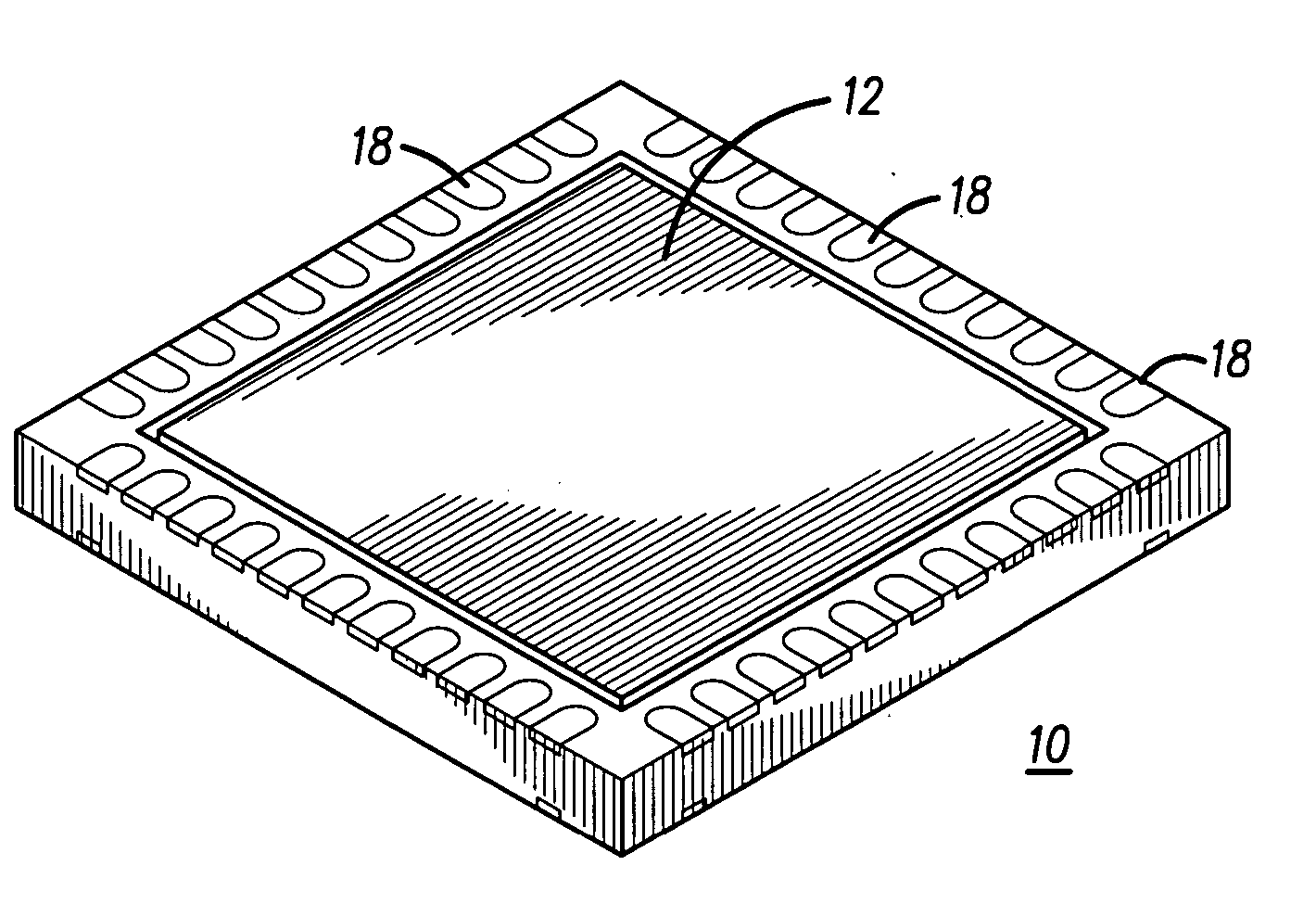
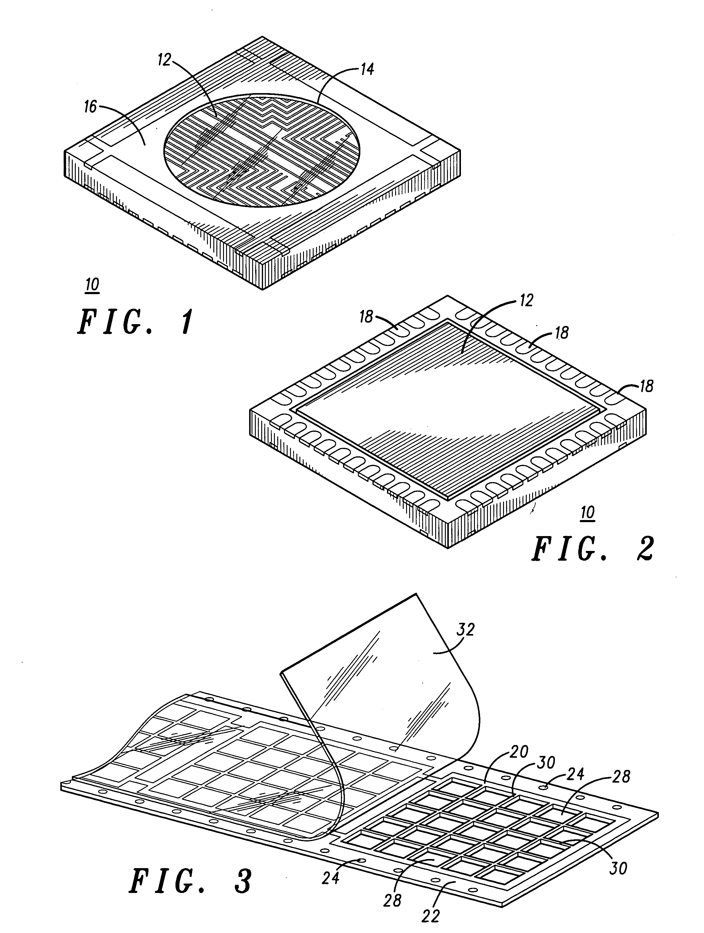
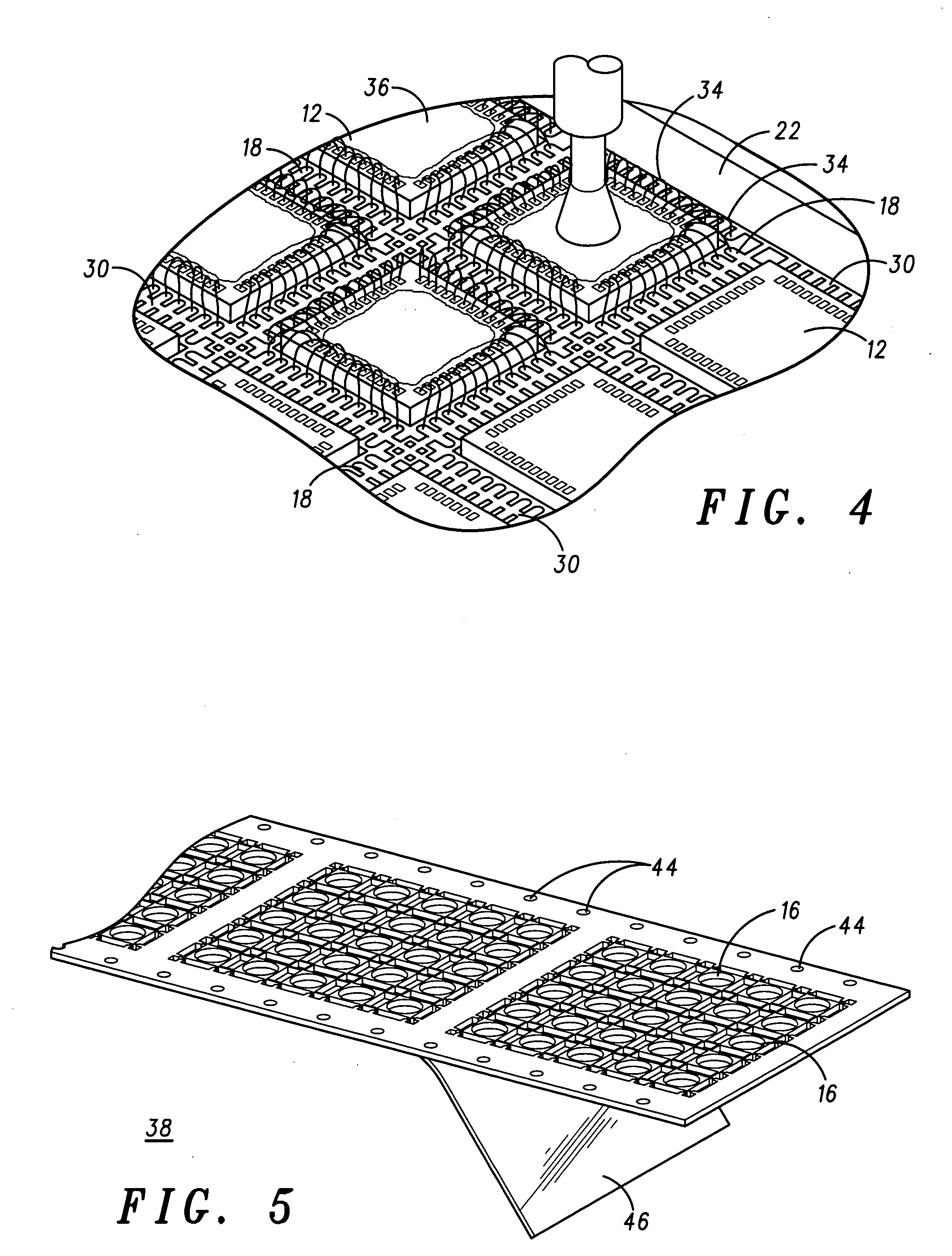
[0018] The present invention provides an image sensor device with low cost and high optical quality in a near chip scale package based on standard high density array format, quad flat no-lead (QFN) assembly in...
PUM
 Abstract
Description
Claims
Application Information