

Method of transporting semiconductor device and method of manufacturing semiconductor device
a technology of semiconductor devices and manufacturing methods, applied in the direction of conveyors, semiconductor/solid-state device details, instruments, etc., can solve the problems of semiconductor chips being liable to easily adhere to the back surface of the upper-stage tray during the handling of the tray, and it is impossible to prevent the occurrence of the adhesion phenomenon of semiconductor chips
- Summary
- Abstract
- Description
- Claims
- Application Information
AI Technical Summary
Benefits of technology
Problems solved by technology
Method used
Image

Examples
embodiment 1
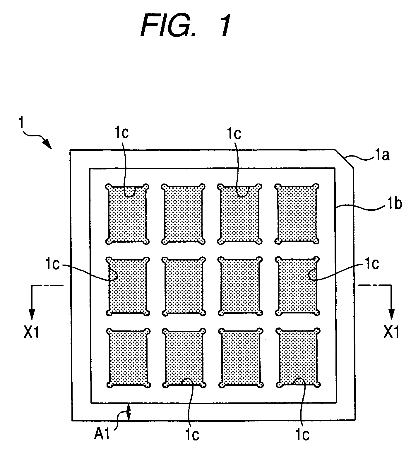
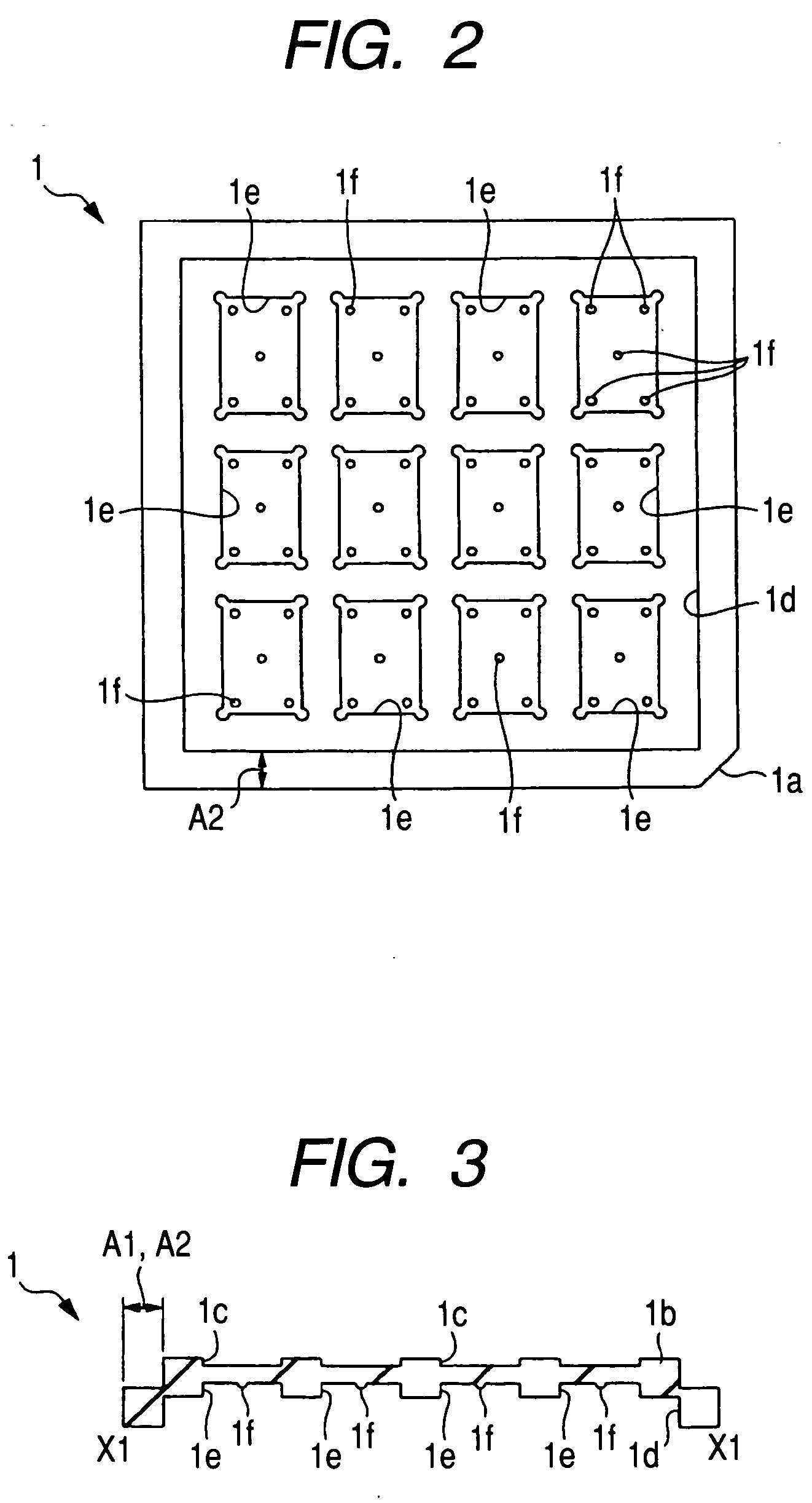
[0083] An example of a tray used in a method of transporting a semiconductor device according to an embodiment 1 is shown in FIG. 1 to FIG. 3. Here, the term transport includes the transport of items for various purposes, such as transport between steps, transport for shipping and the like.
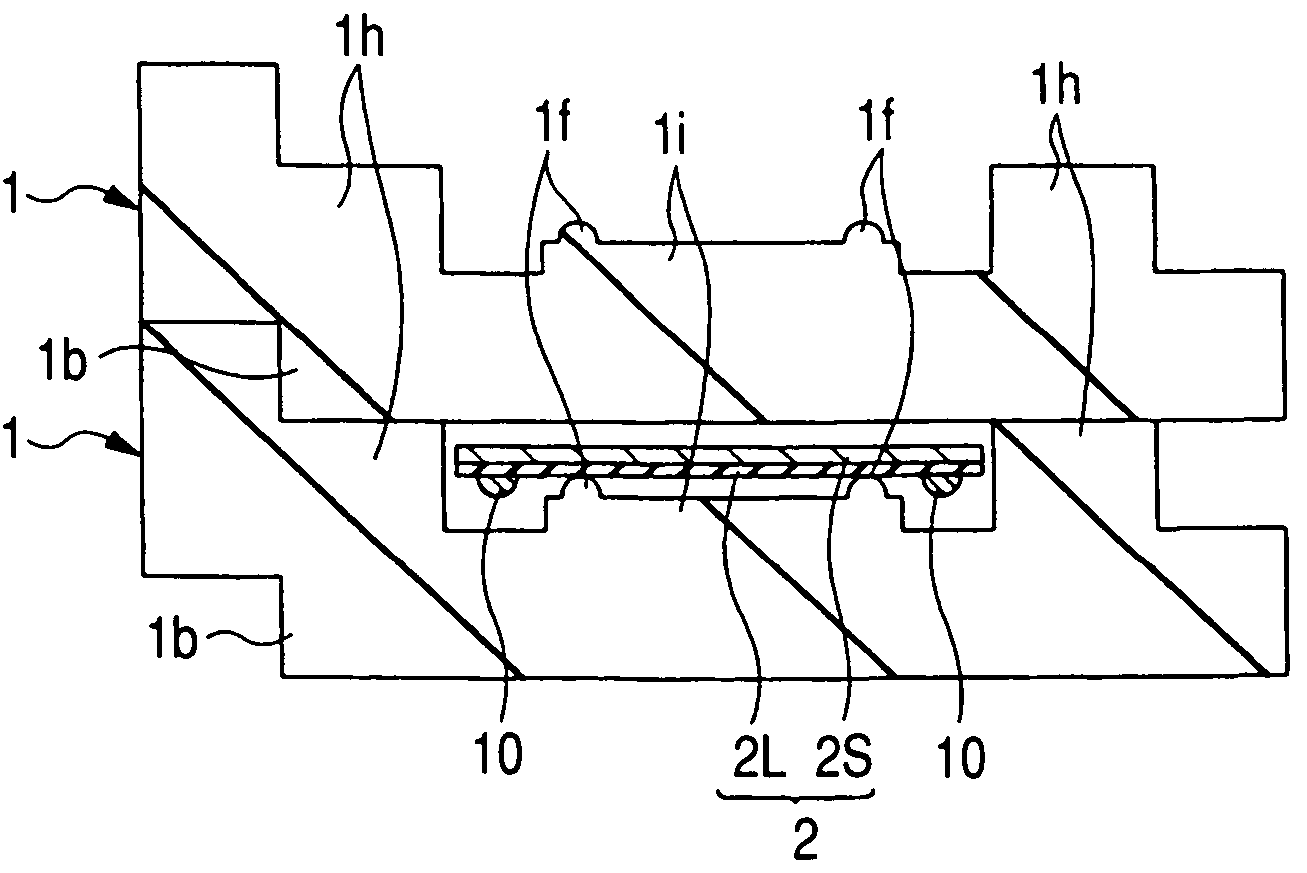
[0084] The tray 1 of this embodiment 1 is a container which is used for transporting semiconductor chips (CSP (Chip Size Package)), for example. The appearance of the tray 1 is configured to have a thin planar approximately square shape, with a chamfered portion 1a for indexing formed in one corner portion thereof, for example. The profile size is set such that the longitudinal size is approximately 50 mm, the lateral width is approximately 50 mm and the height is approximately 4 mm.
[0085] The tray 1 is, for example, made of an insulation material, such as MS (acrylonitrile-acrylate-styrene) resin, ABS (acrylonitrile-butadiene-styrene) resin or PS (polystyrene) resin. From the viewpoint of suppr...
embodiment 2
[0110]FIG. 24 is an overall plan view of a main surface of the tray 1, which is used in a method of manufacture of semiconductor devices which constitutes another embodiment of the present invention, showing trays stacked in two stages, and FIG. 25 is a cross-sectional view taken along a line X4-X4 in FIG. 24.
[0111] In this embodiment 2, a dull finish treatment is not applied to the bottom surfaces of the accommodating portions 1c formed over the main surface of the tray 1. However, in the same manner as the accommodating portions 1e formed over the back surface of the tray 1, projections 1f are formed over the bottom surfaces of the accommodating portions 1c.
[0112] That is, as mentioned previously, in the transport of the semiconductor chips 2 using the trays 1, there may be a case in which it is necessary to take out the semiconductor chip 2 from the tray 1 or to inspect the appearance or the like of the tray 1 in a state in which the stacked body formed by laminating the trays ...
embodiment 3
[0114] First of all, a problem which was originally discovered by the inventors of the present invention is explained. Along with the reduction of the thickness of the semiconductor chips, the chip accommodating portions of the tray which is used for transporting the semiconductor chips are becoming more shallow. However, when the chip accommodating portions are excessively shallow, at the time of placing the semiconductor chip in the chip accommodating portion, or at the time of taking out the semiconductor chip from the chip accommodating portion, there arises a drawback in that the accommodating / takeout operations may influence another semiconductor chip which is already accommodated in another nearby chip accommodating portion, whereby the other semiconductor chip may be expelled to the outside of the chip accommodating portion in which it has been resting. FIG. 26 shows one example of such a drawback, that is, it shows a state in which the semiconductor chip 2 is accommodated i...
PUM
| Property | Measurement | Unit |
|---|---|---|
| height | aaaaa | aaaaa |
| thickness | aaaaa | aaaaa |
| height | aaaaa | aaaaa |
Abstract
Description
Claims
Application Information