Foldover packages and manufacturing and test methods therefor

a technology of microelectronic elements and packaging, applied in the direction of packaging goods, semiconductor/solid-state device details, containers, etc., can solve the problems of high stress level in the adhesive, premature failure of the bond between the adhesive and the tape run, or premature failure of the bond between the adhesive and the die, etc., to reduce the reliability of the package and high stress level

Inactive Publication Date: 2005-07-14
TESSERA INC
View PDF13 Cites 5 Cited by
  • Summary
  • Abstract
  • Description
  • Claims
  • Application Information

AI Technical Summary

Benefits of technology

[0011] One aspect of the present invention incorporates the realization that such a mismatch can reduce the reliability of the package. Although the present invention is not limited by any theory of operation, it is believed that when a tape is formed to a controlled bend radius and hence to a controlled height and the internal unit height is greater than the height of the fold, small, localized bends will be formed at the edges of the internal unit, typically in close proximity to relatively sharp edges on the die or dies. It is believed that such bends and the proximity of the die edges to these bends contribute to premature failure of the traces under conditions involving thermal cycling. If the internal unit height is substantially less than the fold height, it is believed that there will also be small, localized bends in each of the top and bottom runs adjacent the edges of the internal unit. Localized bends of this type are believed to cause high stress levels in the adhesive which bonds the runs of the tape to the internal unit. This, in turn, can lead to premature failure of the bond between the adhesive and the tape runs, or in the bond between the adhesive and the die. Also, where the internal unit height does not match the fold height, the top and bottom runs tend to be non-planar, so that they bulge or droop in the regions between the internal unit and the fold.

Problems solved by technology

It is believed that such bends and the proximity of the die edges to these bends contribute to premature failure of the traces under conditions involving thermal cycling.
Localized bends of this type are believed to cause high stress levels in the adhesive which bonds the runs of the tape to the internal unit.
This, in turn, can lead to premature failure of the bond between the adhesive and the tape runs, or in the bond between the adhesive and the die.

Method used


Image

  • Foldover packages and manufacturing and test methods therefor
  • Foldover packages and manufacturing and test methods therefor
  • Foldover packages and manufacturing and test methods therefor

Examples


Embodiment Construction

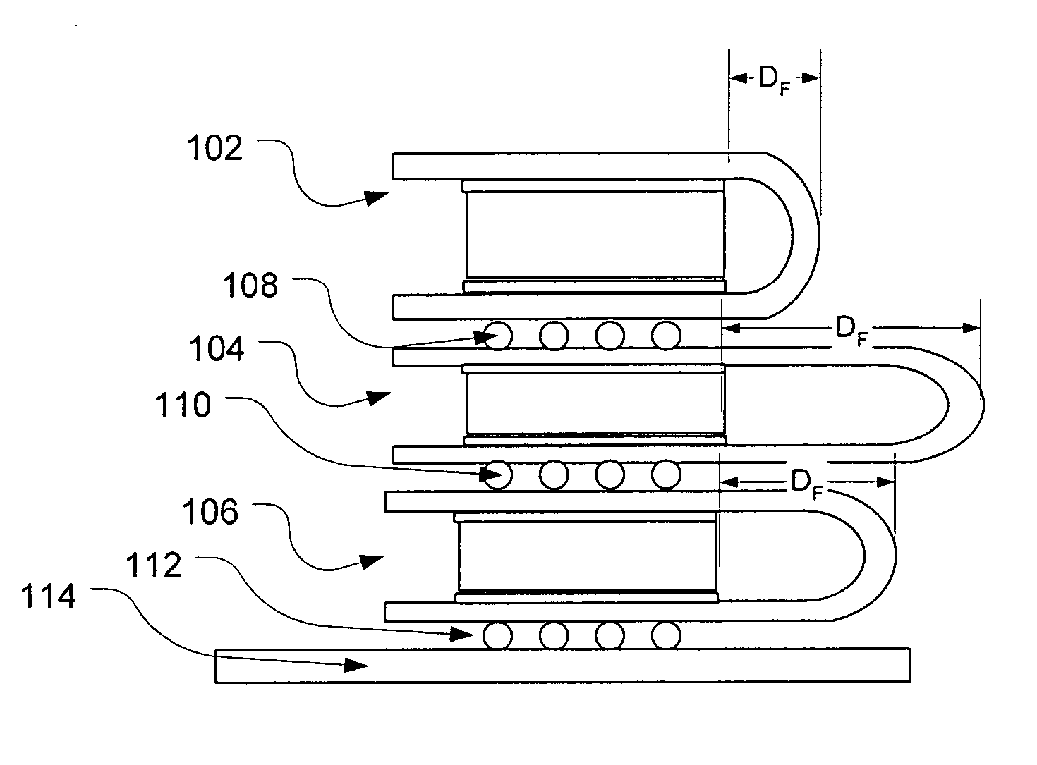
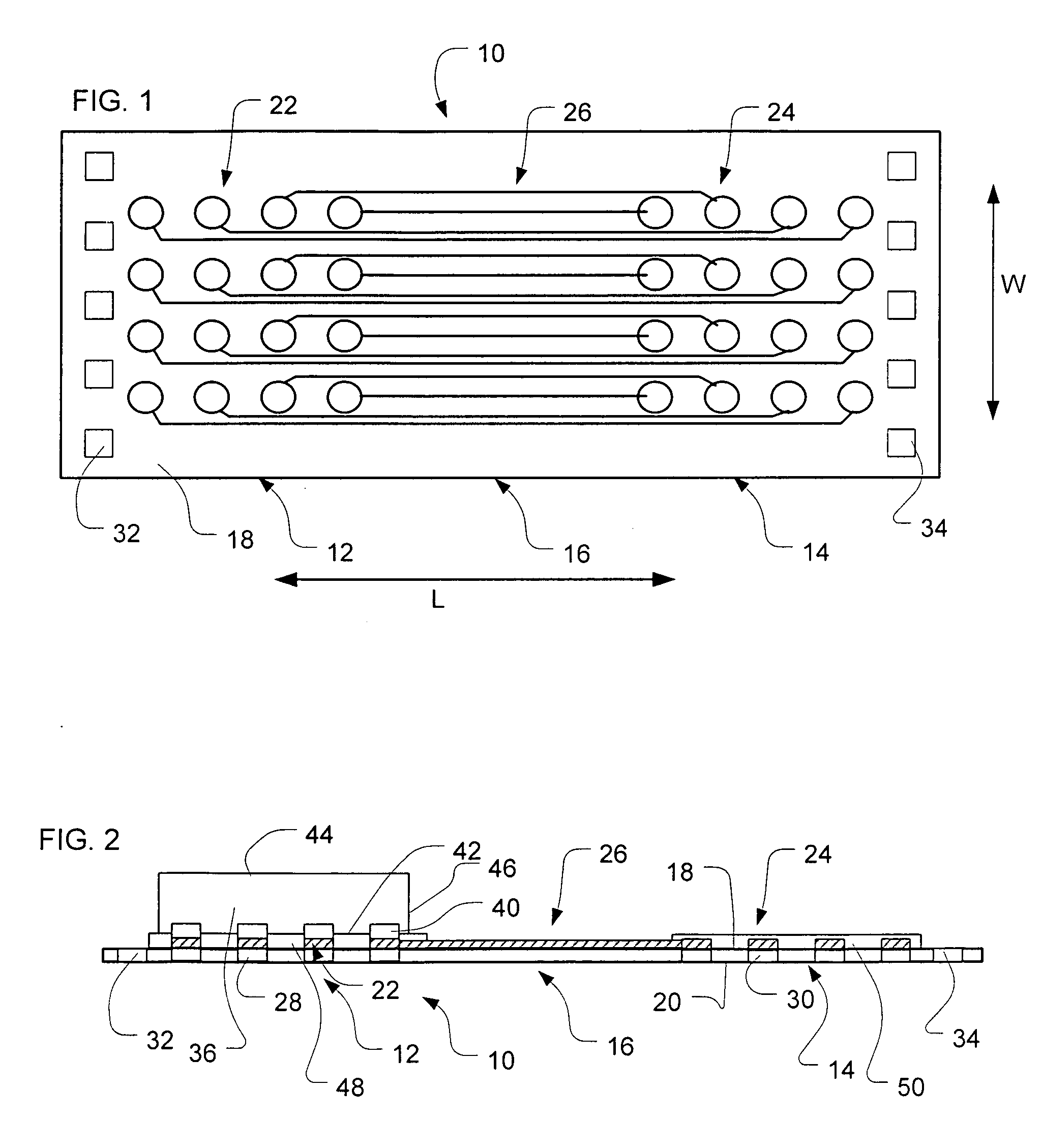
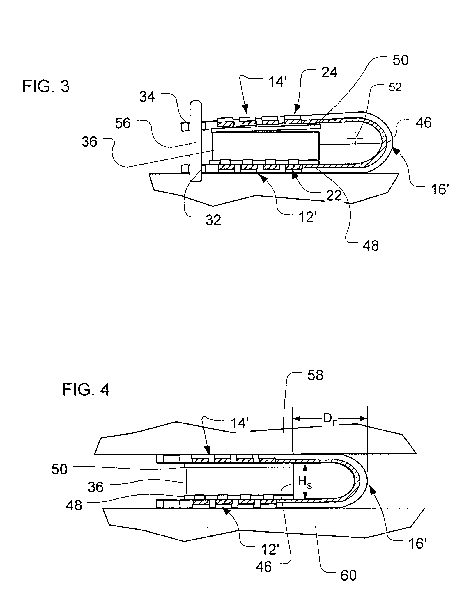
[0023] A process in accordance with one embodiment of the invention utilizes a tape 10 having a first mounting region 12, a second mounting region 14 and a fold region 16 disposed between these end regions. The term “lengthwise direction” is used herein as referring to the direction along the tape between mounting regions 12 and 14, i.e., the direction L from one mounting region to the other across fold region 16. The “widthwise direction” as referred to herein is the direction transverse to the lengthwise direction. Although the terms lengthwise and widthwise are used herein as referring to these directions, this does not imply that the dimension of the tape in the lengthwise direction L must be greater than the dimension of the tape in the widthwise direction.

[0024] The tape includes a dielectric layer having an inner side 18, visible in FIG. 1, and an opposite, outer side 20 (FIG. 2). The dielectric layer may be formed from any material suitable for forming a circuit panel and s...


PUM


Abstract

A microelectronic fold package is formed from an in-process unit including an internal unit such as a chip and a tape defining a bottom run extending beneath the internal unit, a top run extending above the internal unit and a fold connecting said top and bottom runs. The in-process unit is engaged between a pair of elements having flat surfaces so that these elements form the top and bottom runs to a substantially flat condition at least in regions between the internal unit and the fold and so that the engagement elements form the fold to a height equal to the height of the internal unit.

Description

CROSS-REFERENCE TO RELATED APPLICATIONS [0001] The present application claims the benefit of the filing date of U.S. Provisional Patent Application 60 / 515,313, filed Oct. 29, 2004, the disclosure of which is hereby incorporated herein by reference.BACKGROUND OF THE INVENTION [0002] The present invention relates to microelectronic packaging and more particularly relates to fold packages for microelectronic elements, methods of making such packages and methods of testing the same. [0003] Microelectronic elements such as semiconductor chips commonly are provided in packages which protect the chip or other element from physical damage, and which facilitate mounting of the chip on a circuit panel or other element. One type of microelectronic package includes a substrate, also referred to as a “tape” incorporating a dielectric layer such as a layer of a polyimide, BT resin or other polymeric material with electrically conductive features such as terminals on the dielectric element. The ch...

Claims


Application Information

Patent Timeline
Patent Type & Authority Applications(United States)
IPC IPC(8): B65D85/30H01L23/498H01L25/10
CPCH01L23/4985H01L25/105H01L2225/1023H01L2225/1041H01L2924/0002H01L2225/1058H01L2924/00
Inventor THOMPSON, JESSE BURLALFONSO, JENNIFER FOSBERRYURBISH, GLENNOSBORN, PHILIP R.CHAU, ELLIS
Owner TESSERA INC
Why Eureka
Try Eureka