Inclination sensor, method of manufacturing inclination sensor, and method of measuring inclination

a technology of tilt sensor and manufacturing method, which is applied in the field of tilt sensor, can solve the problems of complex manufacturing process, weakening, and increasing costs, and achieves the effect of increasing the size and cost of the cellular phon

Inactive Publication Date: 2005-07-14
ASAHI KASEI ELECTRONICS CO LTD
View PDF7 Cites 47 Cited by
  • Summary
  • Abstract
  • Description
  • Claims
  • Application Information

AI Technical Summary

Benefits of technology

[0019] Thus, it is possible to form a deflectable portion just by grinding the entire backside of the substrate having the piezoresistors formed therein. Therefore, it is no longer necessary to perform selective etching using a photolithographic technology for the purpose of forming a deflectable portion.
[0096] Thus, it is possible to measure the azimuth with comparatively correctly without keeping the cellular phone in a horizontal plane but in a position taken by the user for normal use while curbing increase in the size and the costs of the cellular phone.

Problems solved by technology

Thus, there is a problem that a manufacturing process becomes complicated and costs increase.
Therefore, there is a problem that the tilt sensor has a complicated structure and becomes weak against an impact.
Therefore, there is a problem that the costs increase and it becomes weak against an impact.

Method used


Image

  • Inclination sensor, method of manufacturing inclination sensor, and method of measuring inclination
  • Inclination sensor, method of manufacturing inclination sensor, and method of measuring inclination
  • Inclination sensor, method of manufacturing inclination sensor, and method of measuring inclination

Examples


first embodiment

[0120] Hereinafter, a first embodiment of the present invention will be described by referring to drawings. FIGS. 1A-1C, 2A-2E, 3A-3D, 4A and 4B, 5A and 5B, and 6A-6C are the diagrams showing the first embodiment of a tilt sensor and a manufacturing method thereof according to the present invention.

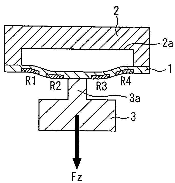
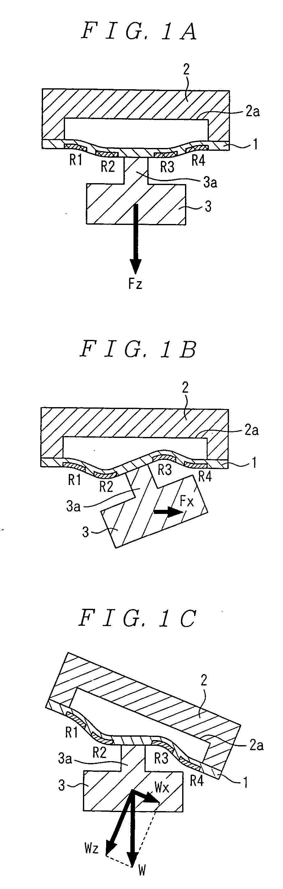
[0121]FIGS. 1A-1C are sectional views showing an operation of the tilt sensor according to an embodiment of the present invention. The embodiment in FIGS. 1A-1C show a configuration of the tilt sensor of a doubly supported structure, where four piezoresistors R1 to R4 are provided on a silicon substrate 1.

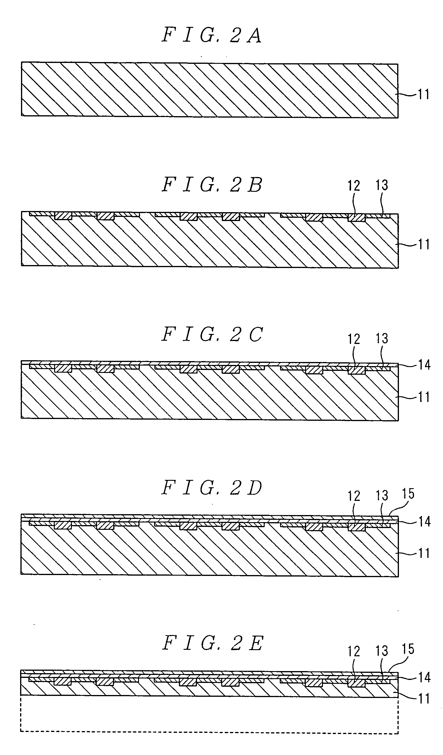
[0122] In FIGS. 1A-1C, the silicon substrate 1 has the piezoresistors R1 to R4 formed on its surf ace, and its backside is uniformly ground to a thickness capable of deflection. And the silicon substrate 1 has a weight member 3 provided at its center by the intermediary of a convex portion 3a.

[0123] The silicon substrate 1 also has a support member 2 having a concave portion 2a provid...

second embodiment

[0162] Next, a second embodiment of the present invention will be described by referring to the drawings. FIGS. 7A-7E are the drawings showing the second embodiment of the tilt sensor and the manufacturing method thereof according to the present invention.

[0163]FIGS. 7A-7E are sectional views showing the manufacturing process of the tilt sensor according to the second embodiment of the present invention. According to the second embodiment, a weight member 33 of the doubly supported structure tilt sensor is arranged by the intermediary of a base 32.

[0164] In FIG. 7A, the base 32 is bonded to the silicon substrate 11 when the processes in FIG. 2A to FIG. 3B are finished. Here, the base 32 is provided to each individual chip cut from the silicon substrate 11, and is arranged to be positioned at the center in the longitudinal direction of each chip.

[0165] As for height of the base 32, it is set so that the surface of the base 32 should be positioned higher than arches of the wires 42...

third embodiment

[0172] Next, a third embodiment of the present invention will be described by referring to the drawings. FIGS. 8A-8E, 9A-9D, 10A and 10B, 11A-11C, and 12 are the drawings showing the third embodiment of the tilt sensor and the manufacturing method thereof according to the present invention.

[0173]FIGS. 8A-8E, 9A-9D, 10A and 10B, 11A-11C, and 12 are sectional views showing the manufacturing process of the tilt sensor according to the third embodiment of the present invention. The third embodiment shows the manufacturing process of a cantilever type tilt sensor.

[0174] In FIG. 8A, a silicon wafer 51 which is about 550 μm thick and of 6-inch diameter is prepared for instance.

[0175] Next, as shown in FIG. 8B, the photolithographic technology is used to selectively ion-implant impurities so as to form piezoresistors 52 on the silicon wafer 51. In fact, the piezoresistors 52 may be mainly comprised of two or more piezoresistive elements.

[0176] And the electrically conductive layer is fo...


PUM


Abstract

A tilt sensor capable of measuring a tilt angle by utilizing piezoresistive effect without selectively etching a substrate having piezoresistors formed therein, wherein the backside of the silicon substrate 1 having piezoresistors R1 to R4 formed therein is uniformly ground to a deflectable thickness, both ends of the silicon substrate 1 are supported by a support member 2, and a weight member 3 is provided at the center of the silicon substrate 1 through a convex portion 3a.

Description

TECHNICAL FIELD [0001] The present invention relates to a tilt sensor and a manufacturing method thereof, and in particular, to the tilt sensor capable of measuring a tilt angle by utilizing a piezoresistive effect without selectively etching a substrate having piezoresistors formed therein, manufacturing method of the tilt sensor and method of measuring the tilt angle. BACKGROUND ART [0002] As for a conventional tilt sensor, there has been a method of measuring a tilt angle based on resistance change in a piezoresistor caused by a stress with tilt angle. [0003]FIG. 76A is a perspective view showing an overview configuration of the conventional tilt sensor, FIG. 76B is a sectional view showing the overview configuration of the conventional tilt sensor, and FIG. 76C is a sectional view showing an enlarged portion of the piezoresistor of the conventional tilt sensor. [0004] In FIGS. 76A to 76C, piezoresistors R are formed on a silicon substrate 201. In an area in which the piezoresist...

Claims


Application Information

Patent Timeline
Patent Type & Authority Applications(United States)
IPC IPC(8): G01C9/06G01C9/12G01P15/08G01P15/12G01P15/18
CPCG01C9/06G01C9/12G01P15/18G01P15/0802G01P15/123G01C2009/068G01P2015/0828G01P2015/084
Inventor HIKIDA, KOICHIYAMASHITA, MASAYAKANAYAMA, YUUICHIFUKUMOTO, HIROFUMI
Owner ASAHI KASEI ELECTRONICS CO LTD
Why Eureka
Try Eureka