Simulation model for design of semiconductor device, thermal drain noise analysis method, simulation method, and simulation apparatus

a simulation model and semiconductor technology, applied in the direction of semiconductor/solid-state device details, optical radiation measurement, instruments, etc., can solve the problems of reducing the size of the mosfet, generating noise has become a serious problem, and the thermal noise is small, so as to accurately estimate the thermal noise

Inactive Publication Date: 2005-07-14
SEMICON TECH
View PDF3 Cites 35 Cited by
  • Summary
  • Abstract
  • Description
  • Claims
  • Application Information

AI Technical Summary

Benefits of technology

[0019] It is, therefore, an object of the present invention to provide a simulation model for the design of a semiconductor device which can accurately estimate thermal noise from the DC characteristics of a MOSFET.

Problems solved by technology

With the recent advances in high integration techniques for semiconductor devices such as ICs and LSIs, the generation of noise has become a serious problem as MOSFETs have been reduced in size. FIG. 1 shows the relationship between a frequency f and a drain current noise spectrum density Sid in MOSFETs manufactured by a 100-nm microfabrication technique.
Thermal noise is, however, small and hence is difficult to directly measure.
As the gate length Lg decreases, thermal noise increases.
It is expected that when the gate length becomes smaller than 0.18 μm, thermal noise will increase more.
Noise generated in a circuit is one parameter that causes a deterioration in circuit characteristics.
As described above, however, thermal noise is small and difficult to measure, and it takes much time to measure it.
In addition, since an apparatus for such measurement is not generally used as compared with that for DC measurement, it is difficult to obtain a parameter on the basis of the measurement result on thermal noise.
As described above, according to the conventional simulation model for the design of a semiconductor device, since calculation is performed with a fixed thermal drain noise coefficient, circuit simulation cannot be done with high precision.
It is, however, difficult to measure thermal noise, and it takes much time to measure it.
It is therefore difficult to obtain a parameter on the basis of the measurement result.
Even if thermal drain noise is measured, it cannot be evaluated or analyzed.
In addition, the conventional semiconductor device simulation method and apparatus using this model cannot accurately simulate the electrical characteristics or circuit operation of a semiconductor device formed from microfabricated MOSFETs.

Method used


Image

  • Simulation model for design of semiconductor device, thermal drain noise analysis method, simulation method, and simulation apparatus
  • Simulation model for design of semiconductor device, thermal drain noise analysis method, simulation method, and simulation apparatus
  • Simulation model for design of semiconductor device, thermal drain noise analysis method, simulation method, and simulation apparatus

Examples


Embodiment Construction

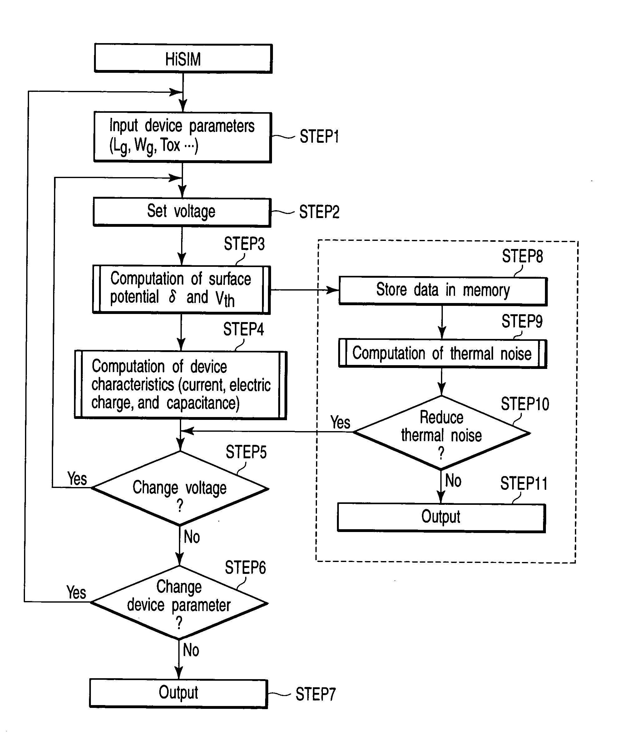
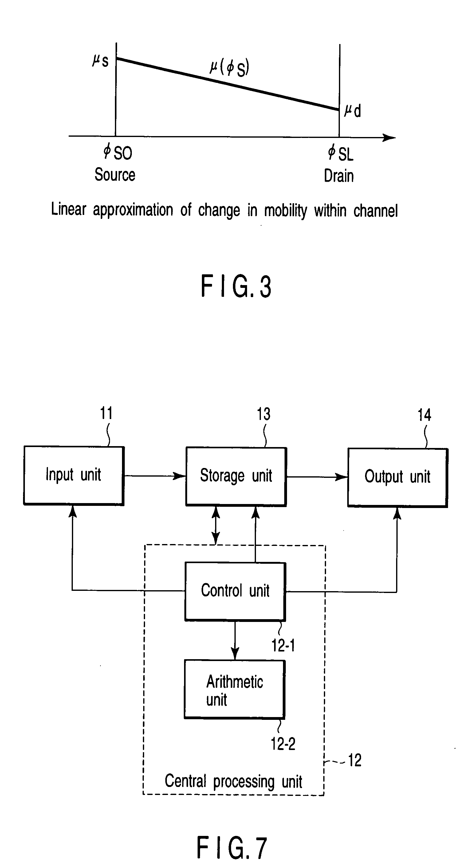
[0040] A simulation model for the design of a semiconductor device will be described first. An example of a simulation method and apparatus which use this simulation model will be described next.

(A) Derivation of Basic Equation for

[0041] Thermal Drain Noise

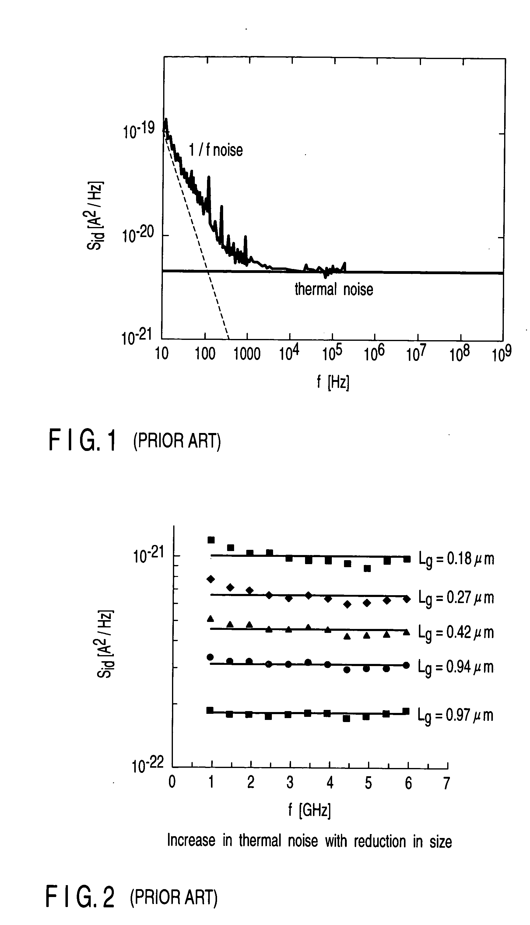
[0042] First of all, a basic equation is derived from a thermal noise model based on the H. Nyquist theorem (H. Nyquist, Phys. Rev., 32, 110, 1928, “Thermal Agitation of Electric Charge in Conductors”): Sid=1L2⁢∫0L⁢4⁢k⁢ ⁢T⁢ ⁢gds⁡(x)⁢ⅆx(4)

[0043] In a MOSFET, letting φs be the potential at a distance x from a source terminal, and gds(x) be the small channel conductance, gds(x) can be expressed in terms of a function gds(φs) of φs. Since the drain current is expressed as Ids=gds⁡(ϕs)⁢ ⁢ⅆϕsⅆx(5)

the integration of the two sides within the channel yields Ids=1L⁢ ⁢∫ϕSOϕSL⁢gds⁡(ϕS)⁢ⅆϕS(6)

where φs0 and φsL represent the surface potentials at the source terminal and drain terminal in the channel.

[0044] According to equation (5) as...


PUM


Abstract

A semiconductor device simulation method includes the step of storing, in a storage unit, a surface potential and threshold voltage obtained by computation, the step of computing thermal drain noise on the basis of the data of the surface potential and thermal drain noise stored in the storage unit, and the step of determining whether or not to reduce thermal drain noise, and reflecting the computation result in simulation of the model when it is determined that thermal drain noise is to be reduced. A drain current Ids of a MOSFET is calculated and substituted into a relational expression for a drain current noise spectrum density obtained from a Nyquist theorem equation, thereby calculating a thermal drain noise coefficient γ of the MOSFET by substituting the current Ids into a relational expression for a thermal drain noise spectrum density which is obtained from the Nyquist logical equation.

Description

CROSS-REFERENCE TO RELATED APPLICATIONS [0001] This application is based upon and claims the benefit of priority from prior Japanese Patent Application No. 2003-420845, filed Dec. 18, 2003, the entire contents of which are incorporated herein by reference. BACKGROUND OF THE INVENTION [0002] 1. Field of the Invention [0003] The present invention relates to a simulation model for the design of a semiconductor device which is used to estimate thermal drain noise from the DC characteristics of a MOSFET, a thermal drain noise analysis method using the model, and a simulation method and apparatus which simulate the electrical characteristics or circuit operation of a semiconductor device on a computer by means of the model. [0004] 2. Description of the Related Art [0005] With the recent advances in high integration techniques for semiconductor devices such as ICs and LSIs, the generation of noise has become a serious problem as MOSFETs have been reduced in size. FIG. 1 shows the relations...

Claims


Application Information

Patent Timeline
Patent Type & Authority Applications(United States)
IPC IPC(8): G01J5/00G06F7/60G06F17/10G06F17/50G06G7/62H01L21/336H01L21/66H01L23/58H01L29/00H01L29/78
CPCG06F17/5036H01L2924/0002H01L2924/00G06F30/367
Inventor MIURA, MITIKOUENO, HIROAKIHOSOKAWA, SATOSHI
Owner SEMICON TECH
Why Eureka
Try Eureka