Semiconductor device provided with temperature detection function

a technology of semiconductor devices and functions, applied in the direction of pulse techniques, basic electric elements, electronic switching, etc., can solve the problems of unwanted surge current affecting the elements of semiconductor devices, and achieve the effect of increasing the esd resistance of the temperature detection diode and high temperature detection accuracy

Inactive Publication Date: 2005-07-21
TOYOTA IND CORP
View PDF9 Cites 31 Cited by
  • Summary
  • Abstract
  • Description
  • Claims
  • Application Information

AI Technical Summary

Benefits of technology

[0007] The present invention provides a semiconductor device provided with a temperature detection function that increases the ESD resistance of the temperature detection diode and has a high temperature detection accuracy.

Problems solved by technology

The surge current may affect the elements of the semiconductor device in an undesirable manner.

Method used


Image

  • Semiconductor device provided with temperature detection function
  • Semiconductor device provided with temperature detection function
  • Semiconductor device provided with temperature detection function

Examples


Embodiment Construction

[0022] In the drawings, like numerals are used for like elements throughout.

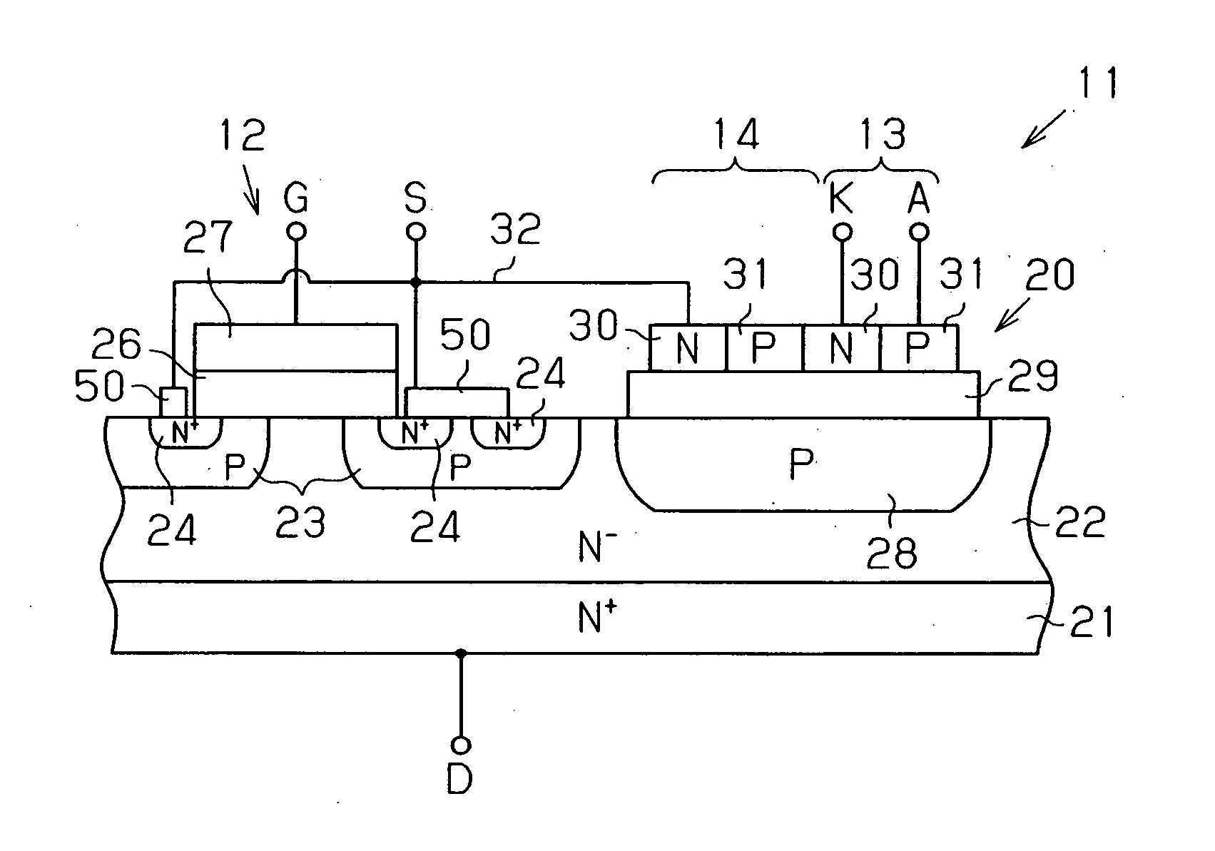
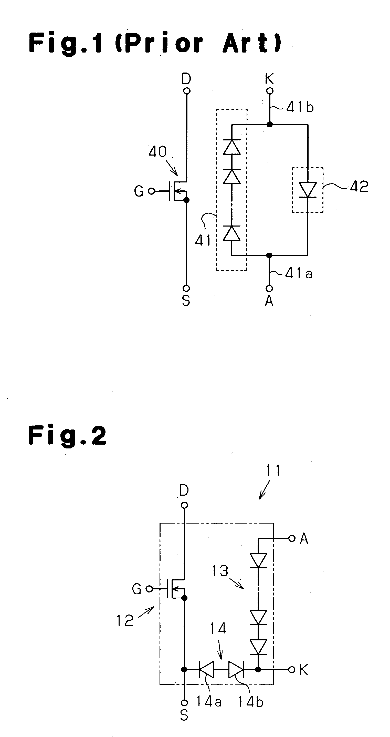
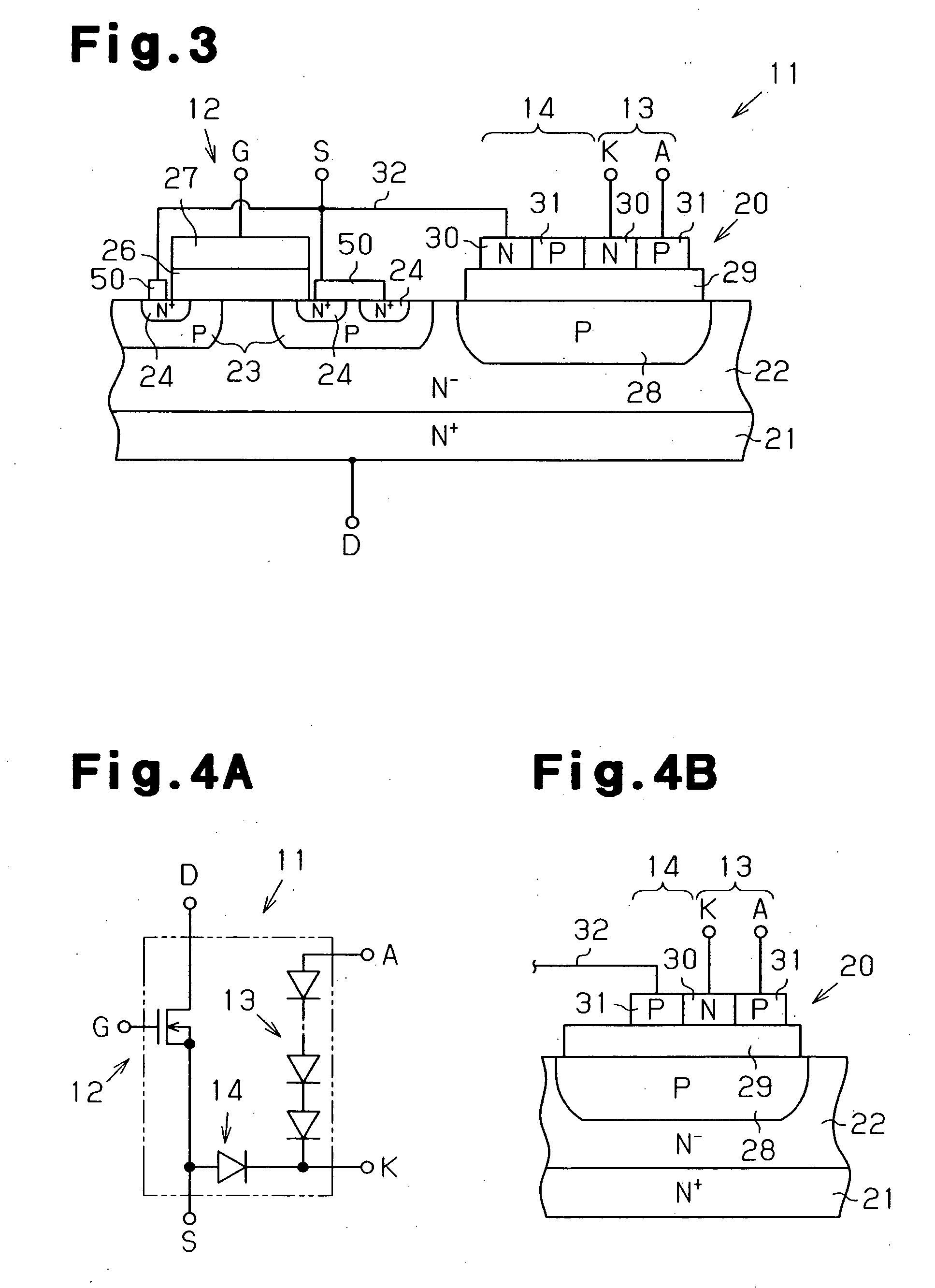
[0023] A semiconductor device 11 according to a preferred embodiment of the present invention will now be discussed with reference to FIGS. 2 and 3. The semiconductor device 11 is provided with a temperature detection function and includes an N-channel MOSFET 12. FIG. 2 is an equivalent circuit diagram of the semiconductor device 11, and FIG. 3 is a schematic, partial cross-sectional diagram of the semiconductor device 11.

[0024] Referring to FIG. 2, the semiconductor device 11 includes the N-channel MOSFET 12 (semiconductor element), a temperature detection diode group 13, and a protection diode group 14. The protection diode group 14 is connected between the source S of the MOSFET 12 and the cathode K of the temperature detection diode group 13. When the MOSFET 12 is activated, either one of the source S or drain D functions as the ground side of the MOSFET 12. Thus, the protection diode group 14 is conne...


PUM


Abstract

A semiconductor device provided with a temperature detection function having a high temperature detection accuracy for improving the ESD resistance of a temperature detection diode. The semiconductor device has a semiconductor element. A temperature detection diode is used to detect the temperature of the semiconductor element and an ambient temperature of the semiconductor element. A protection diode is connected between a cathode of the temperature detection diode and a ground side of the semiconductor element when the semiconductor element is activated.

Description

BACKGROUND OF THE INVENTION [0001] The present invention relates to a semiconductor device, and more specifically, to a semiconductor device provided with a function for detecting the temperature of a semiconductor element or the ambient temperature of a semiconductor element. [0002] Japanese Patent No. 2630242 describes an example of a semiconductor device that prevents breakage of a semiconductor element when the temperature of the activated semiconductor element increases to an abnormal level. The semiconductor device includes a heat sensing element in addition to the semiconductor device. When there is an abnormal increase in the temperature of the semiconductor device, the heat sensing element detects the temperature increase and generates a detection signal. The semiconductor device deactivates the semiconductor element in response to the detection signal to avoid thermal breakage. [0003] Referring to FIG. 1, the semiconductor device includes a MOS transistor 40 and a diode 41...

Claims


Application Information

Patent Timeline
Patent Type & Authority Applications(United States)
IPC IPC(8): H01L21/822H01L23/34H01L23/62H01L27/02H01L27/04H01L27/06H01L29/78H03K17/08
CPCH01L23/34H01L27/0248H01L29/7395H01L29/7804H01L2924/0002H01L29/7808H01L2924/00
Inventor MORI, SHOGOONO, KENJI
Owner TOYOTA IND CORP
Why Eureka
Try Eureka