Planar electron emitter apparatus with improved emission area and method of manufacture

a technology of electron emitter and emission area, which is applied in the manufacture of electrode systems, electric discharge tubes/lamps, and discharge tubes luminescnet screens, etc., can solve the problems of high-vacuum, high cost, and difficult to achieve high-vacuum, and achieve the effect of improving the electron emission ra

Inactive Publication Date: 2005-07-21
HEWLETT PACKARD DEV CO LP
View PDF4 Cites 37 Cited by
  • Summary
  • Abstract
  • Description
  • Claims
  • Application Information

AI Technical Summary

Problems solved by technology

Further, the manufacturing steps necessary to produce and fabricate field tip emitters is extremely complex.
High-vacuums are expensive and difficult to achieve.
This is not desired due to significant curvature of electric field lines in that region which causes the beam to become divergent rather than primarily collimated.

Method used


Image

  • Planar electron emitter apparatus with improved emission area and method of manufacture
  • Planar electron emitter apparatus with improved emission area and method of manufacture
  • Planar electron emitter apparatus with improved emission area and method of manufacture

Examples


Embodiment Construction

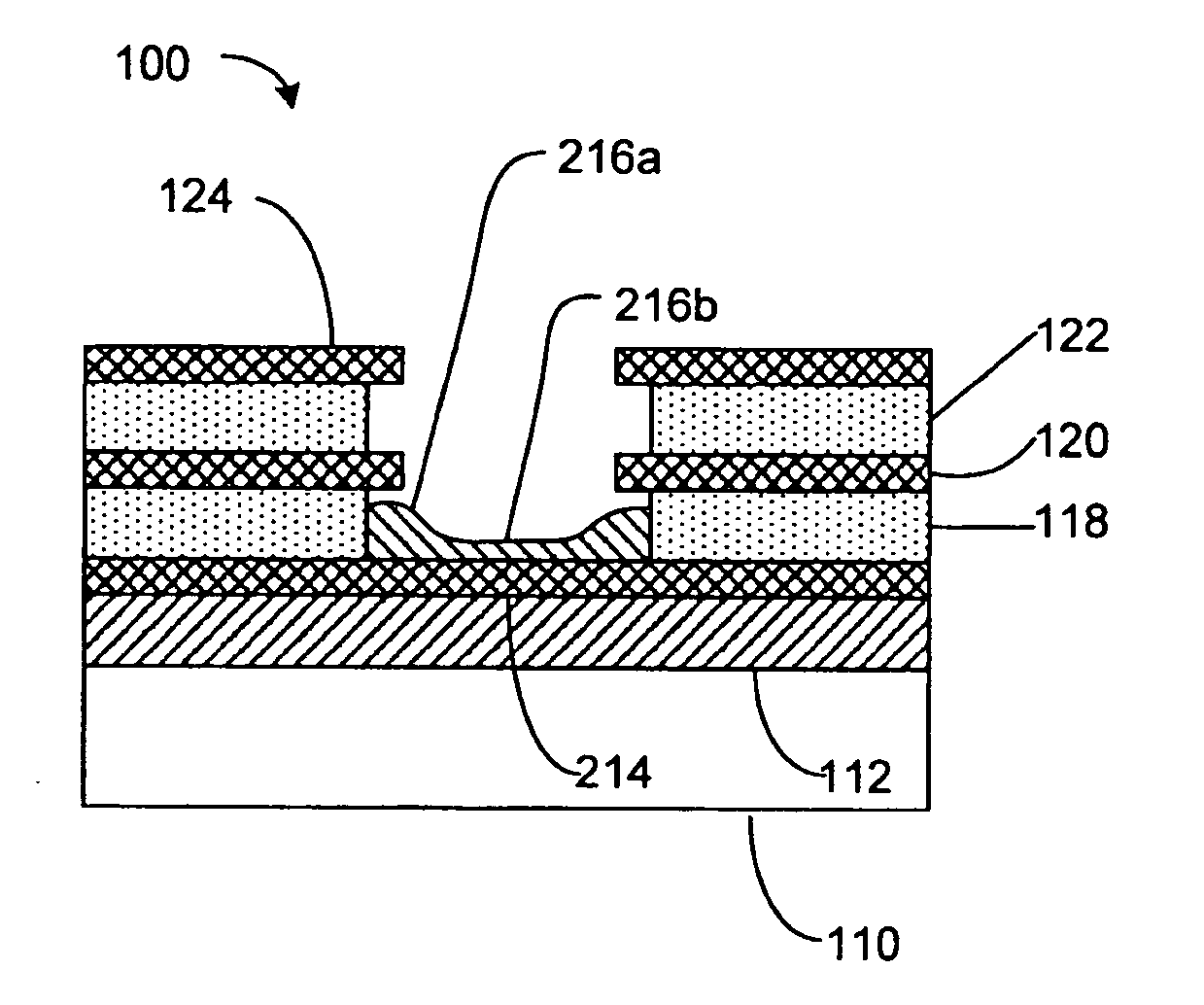
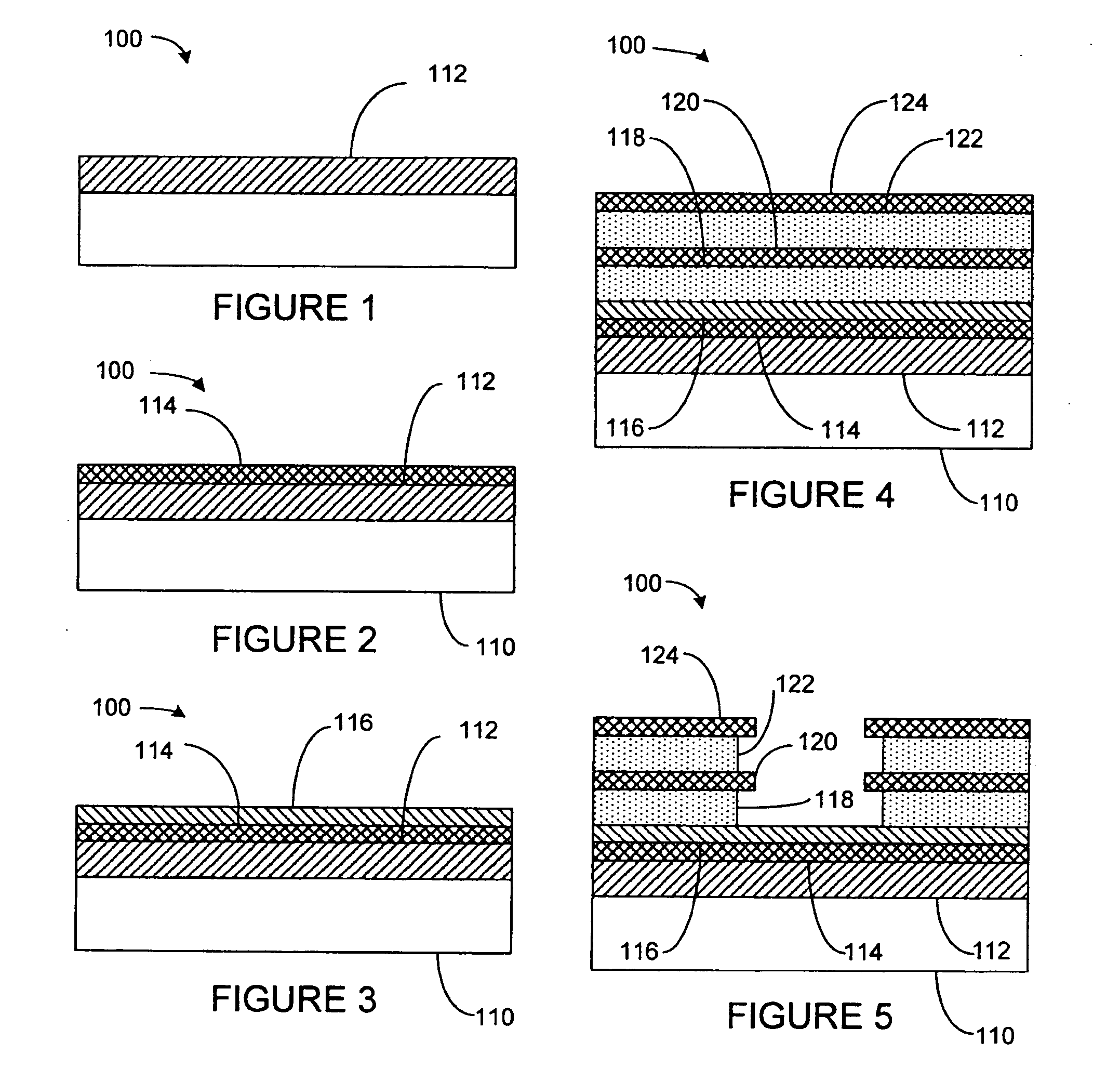
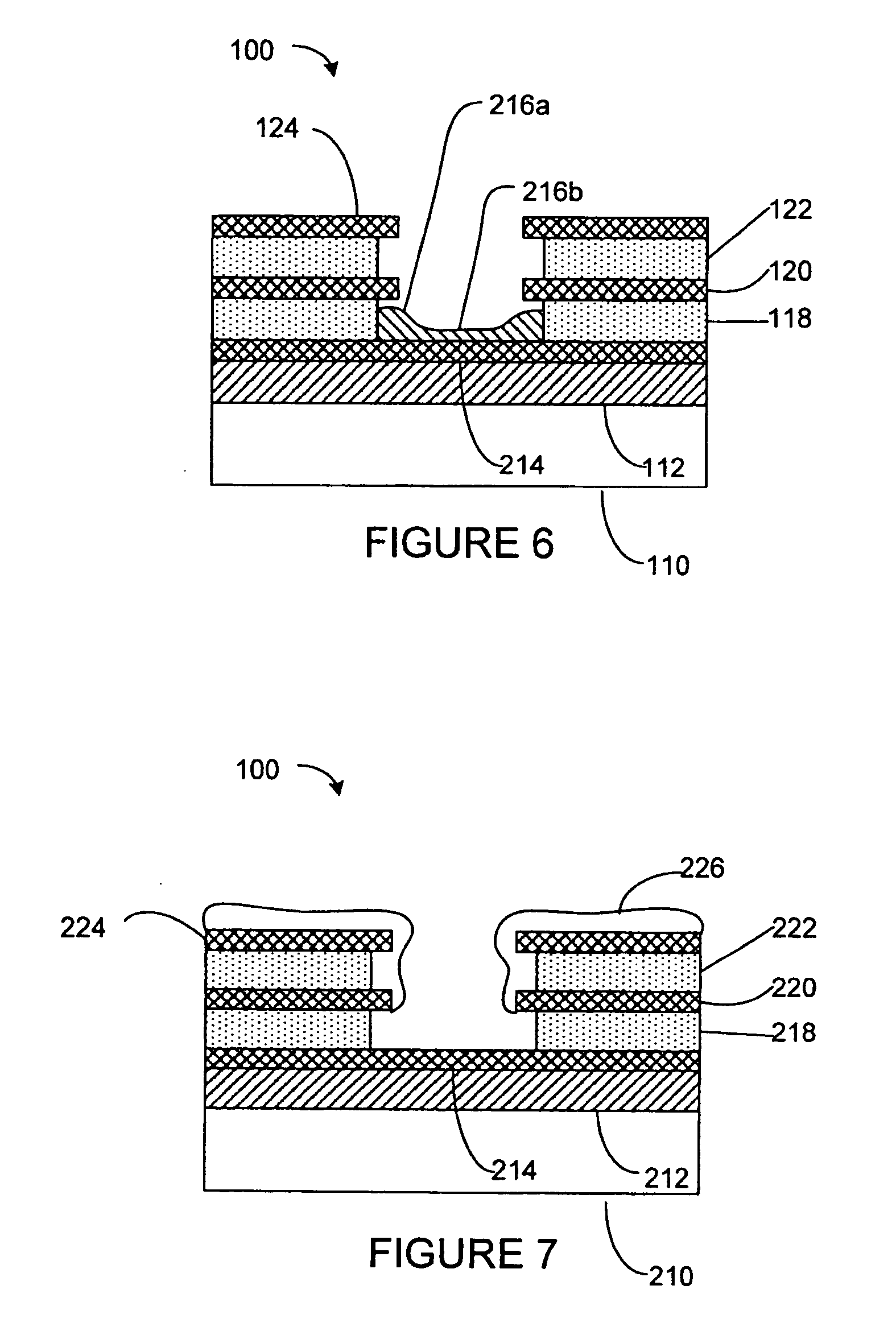
[0021] An improved planar field emission electron emitter structure that is typically utilized within an ultra-high density storage device is disclosed in FIGS. 1-5. The emitter structure 100 utilizes a solid state mechanism to enhance and improve electron emission for use in structures such as ultra-high density storage devices, previously disclosed in U.S. Pat. No. 5,557,596, incorporated by reference for all purposes, and in field emission-based display systems such as the type disclosed in U.S. Pat. No. 5,587,628, incorporated by reference for all purposes. The structure is also based on the structure described and illustrated in WO 00 / 70638, published Nov. 23, 2000, as well as French patent No. FR9906254.

[0022] The solid state mechanism utilizes a thin metal layer placed upon the emitter electrode of the planar field emission electron emitter device. Next, a thin layer of wide band-gap semiconductor material is placed upon the metal layer, which forms a Schottky metal-semicond...


PUM

PropertyMeasurementUnit
thicknessaaaaaaaaaa
thicknessaaaaaaaaaa
thicknessaaaaaaaaaa

Abstract

The field emission planar electron emitter device is disclosed that has an emitter electrode, an extractor electrode, and a planar emitter emission layer, electrically coupled to the emitter electrode and the extractor electrode. The planar electron emitter is configured to bias electron emission in a central region of the emission layer in preference to an outer region thereof. One structural example that provides this biasing is achieved by fabricating the planar emitter emission layer so that it has an outer perimeter that is thicker in depth than at an interior portion of the planar emitter emission layer, which reduces electron beam emission at the outer perimeter when an electric field is applied between the emitter electrode and the extractor electrode. The electric field draws emission electrons from the surface of the planar emitter emission layer towards the extractor electrode at a higher rate at the interior portion than at the outer perimeter. The planar electron emitter device further includes a focusing electrode electrically coupled to the planar electron emitter.

Description

BACKGROUND OF THE INVENTION [0001] Another application in emitter devices is described in commonly assigned, co-pending U.S. patent application No. ______ (HP docket number 10004242-1), entitled “IMPROVED ELECTRON EMITTER DEVICE FOR DATA STORAGE APPLICATIONS AND METHOD OF MANUFACTURE”, the disclosure of which is hereby incorporated herein by reference. [0002] The present invention relates generally to emitter devices utilized in ultra-high density memory storage systems, and more particularly, the present invention relates to an improved solid state emitter that optimizes electron emission in a central location to improve focusing accuracy. [0003] Memory storage systems have made tremendous advancements over the years from the first use of magnetic tape to magnetic hard drives and now optical drives as well as sophisticated fast memory such as S-RAM and D-RAM. A more recent development has utilized field emission electron emitters within an ultra-high density storage device. The fie...

Claims


Application Information

Patent Timeline
Patent Type & Authority Applications(United States)
IPC IPC(8): H01J1/304G11B9/10H01J1/308H01J1/312
CPCB82Y10/00H01J1/312H01J1/308G11B9/10
Inventor BIRECKI, HENRYKBINH, VU THIEN
Owner HEWLETT PACKARD DEV CO LP
Why Eureka
Try Eureka