Display device and display unit using the same

Inactive Publication Date: 2005-07-28
SONY CORP
View PDF4 Cites 4 Cited by
  • Summary
  • Abstract
  • Description
  • Claims
  • Application Information

AI Technical Summary

Benefits of technology

[0008] As described above, according to the present invention, since a display device is modularized by burying a light emitting device finely formed in an insulating material so as to re-shape the light emitting device into a size easy to handle, it is possible to reduce the production cost of the display device as much as possible, to ensure the handling performance thereby and to

Problems solved by technology

Such a production method is disadvantageous in that since not only packaging of each LED requires a large production cost but also carrying

Method used


Image

  • Display device and display unit using the same
  • Display device and display unit using the same
  • Display device and display unit using the same

Examples


Embodiment Construction

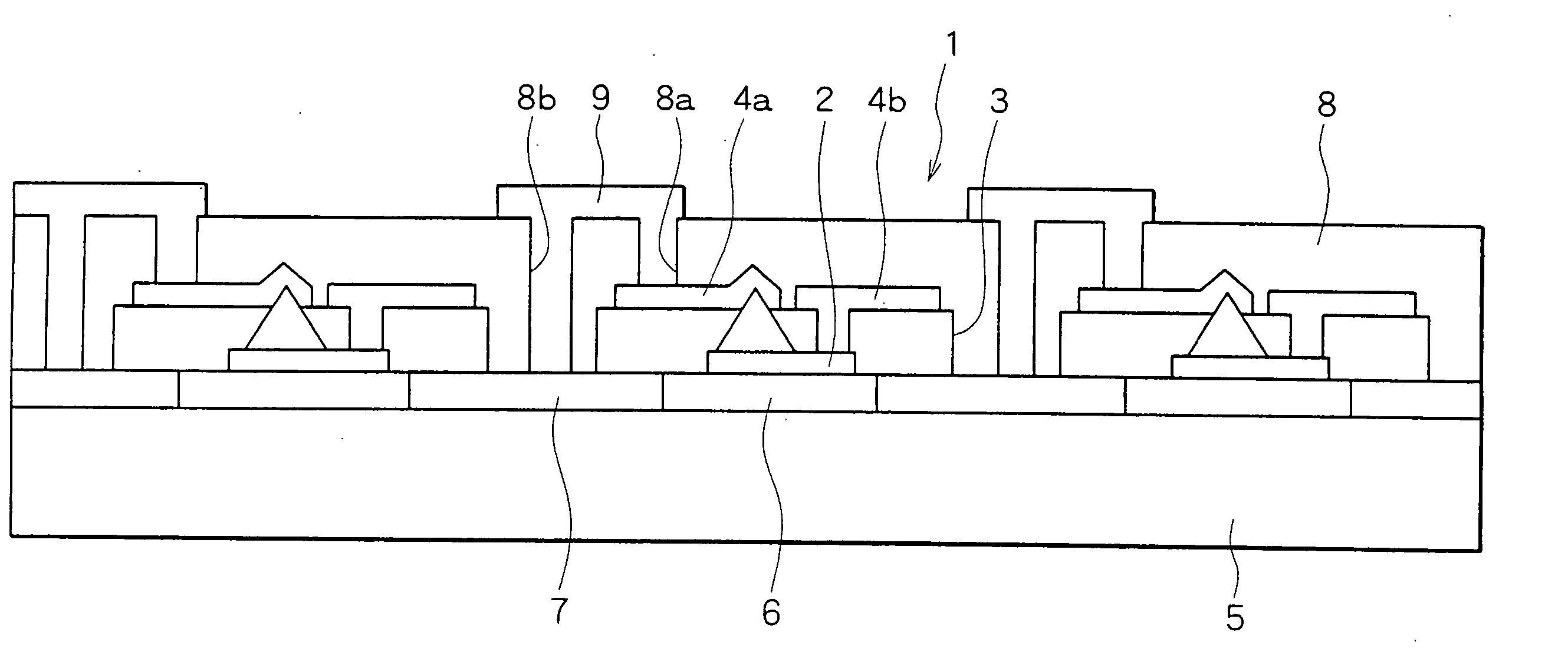
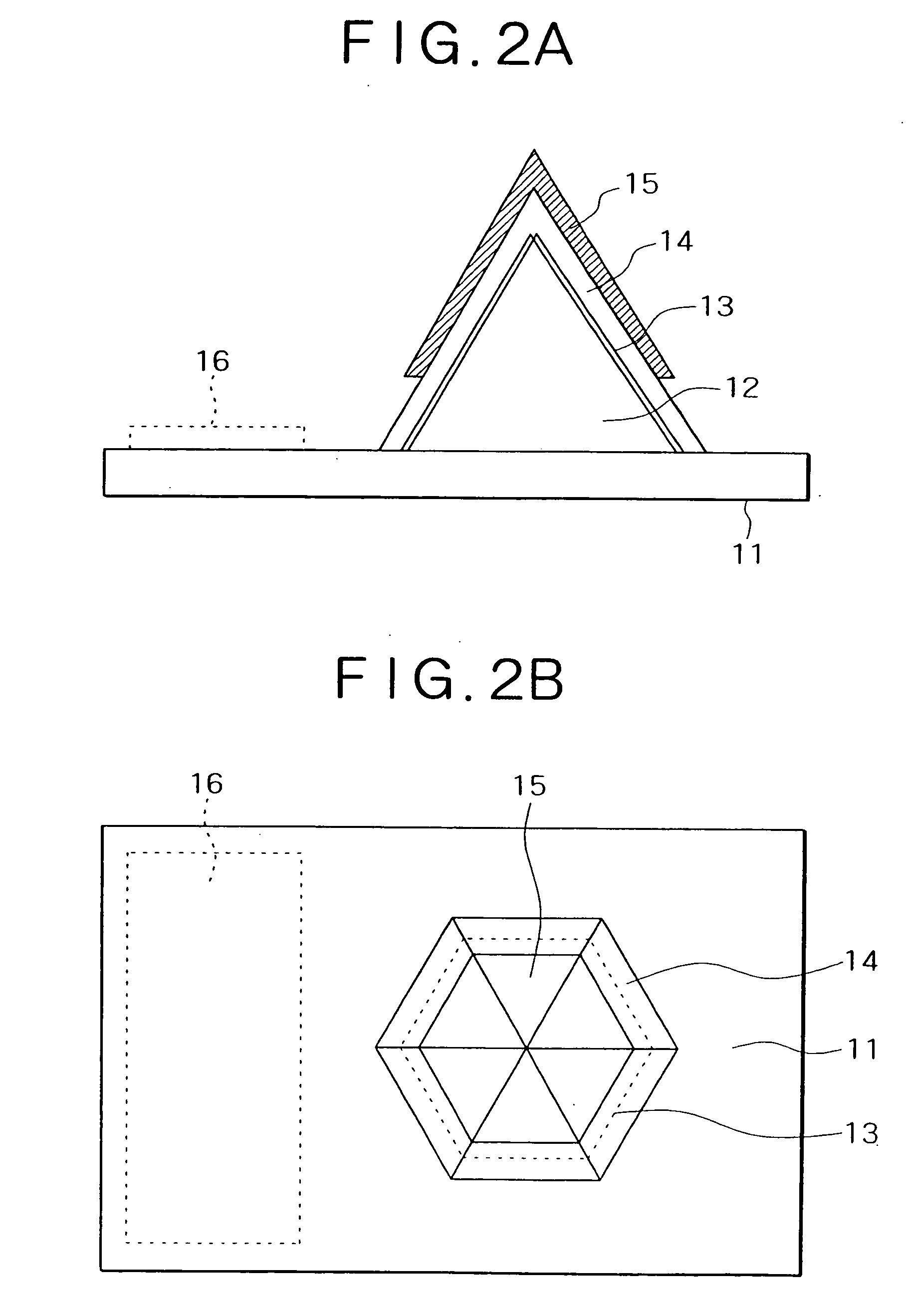
[0025] Basic Structure of Display Device:

[0026] A display device 1 of the present invention has a configuration shown in FIG. 1, in which a light emitting device 2 is buried in an insulating material 3 such as polyimide resin or epoxy resin, and drive electrodes 4a and 4b are formed on surfaces of the insulating material 3. The light emitting device 2 has a shape whose sides converge in one direction, that is, includes a leading end portion 2a having a taper shape, for example, a conical shape or a polygonal pyramid shape. The leading end portion 2a is exposed from the insulating material 3, and the drive electrode 4a is connected to the exposed portion (p-electrode) of the leading end portion 2a. The other drive electrode 4b is connected to the other electrode (n-electrode) of the light emitting device 2 via an opening portion 3a formed in the insulating material 3.

[0027] The light emitting device 2 is configured as a GaN based light emitting diode formed; for example, on a sapph...


PUM


Abstract

A display device is formed by burying at least part of a light emitting device in an insulating material, wherein a drive electrode for the light emitting device is formed so as to be extracted on a surface of the insulating material. A display unit is produced by two-dimensionally arraying such light emitting devices on a base body. Since the display device is modularized by burying a light emitting device finely formed in an insulating material, to re-shape the light emitting device into a size easy to handle, it is possible to suppress the production cost of the display unit using such display devices, and to ensure a desirable handling performance of the light emitting device; for example, facilitate the carrying of the light emitting device or the mounting thereof on a base body.

Description

BACKGROUND OF THE INVENTION [0001] The present invention relates both to a new display device modularized by burying a light emitting device in an insulating material, and to a display unit produced by two-dimensionally arraying such display devices. [0002] In the case of assembling an image display unit by arraying light emitting devices in a matrix, if the image display unit is a liquid crystal display (LCD) or a plasma display panel (PDP), then light emitting devices have been directly formed on a substrate, while if the image display unit is a light emitting diode (LED) display, then single LED packages are arrayed on a substrate. For example, in the case of producing an image display unit such as an LCD or PDP, device isolation is impossible from the viewpoint of its structure and, accordingly, devices generally have been formed, at the beginning of the production process, in such a manner as to be spaced from each other with a pitch equivalent to a pixel pitch of a final image...

Claims


Application Information

Patent Timeline
IPC IPC(8): G09F9/33G09F9/00H01L25/075H01L27/15H01L33/16H01L33/24H01L33/32H01L33/56
CPCH01L25/0753H01L27/156H01L33/24H01L2924/0002H01L2924/00
Inventor OOHATA, TOYOHARUNAKAJIMA, HIDEHARUYANAGISAWA, YOSHIYUKIIWAFUCHI, TOSHIAKI
Owner SONY CORP
Why Eureka
Try Eureka