Organic electro luminescence device

a luminescence device and organic technology, applied in the direction of luminescence screens, discharge tubes, instruments, etc., can solve the problems of reducing the life span of the organic electro luminescence device, and achieve the effects of improving dc reliability, increasing width-to-length ratio (w/l), and high definition

Active Publication Date: 2005-07-28
LG DISPLAY CO LTD
View PDF10 Cites 11 Cited by
  • Summary
  • Abstract
  • Description
  • Claims
  • Application Information

AI Technical Summary

Benefits of technology

[0017] An object of the present invention is to provide an organic electro luminescence device that has a driving thin film transistor having an increased width-to-length ratio (W / L), thereby obtaining a higher definition.
[0018] Another object of the present invention is to provide an organic electro luminescence device that has a driving thin film transistor having source and drain electrodes in a comb shape with a plurality of vertical protrusions, thereby obtaining an improved DC reliability and better product life span.

Problems solved by technology

As a result, current density applied to the organic electro luminescence layer is relatively high, and the drive TFT TD experiences DC stress for many hours, thereby reducing the life span of the organic electro luminescence device.

Method used


Image

  • Organic electro luminescence device
  • Organic electro luminescence device
  • Organic electro luminescence device

Examples


Embodiment Construction

[0032] Reference will now be made in detail to the preferred embodiments, examples of which are illustrated in the accompanying drawings.

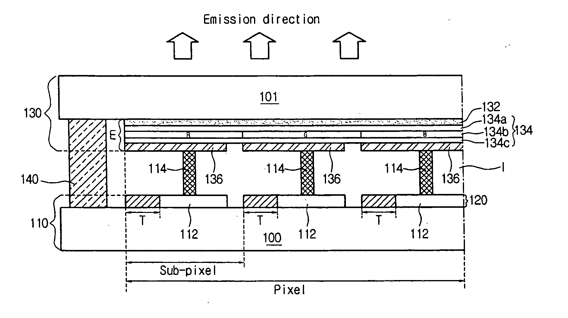
[0033]FIG. 4 is a schematic sectional view of a dual panel type organic electro luminescence device according to an embodiment of the present invention. However, the present invention is not limited to the dual panel type. In FIG. 4, an organic electro luminescent device may include first and second substrates 110 and 130 arranged facing each other with a predetermined gap I therebetween. The first and second substrates 110 and 130 may be attached to each other by a seal pattern 140 along edges of the first and second substrates 110 and 130.

[0034] In addition, an array element 120 may be formed on a transparent substrate 100 of the first substrate 110. The array element 120 may include a thin film transistor (TFT) T and an electric connecting portion 112 connected to the TFT T. The electric connecting portion 112 may extend from an electrode defi...


PUM


Abstract

An organic electro luminescence device includes a gate line, a data line intersecting the gate line and defining a pixel area, a power line parallel to the data line, and an array element formed in the pixel area and corresponding to an organic electro luminescence diode, the array element including a switching TFT, a drive TFT and a storage capacitor, and the drive TFT including source and drain electrodes, one of the source and drain electrodes having at least one vertical protrusion, and another of the source and drain electrodes having at least two vertical protrusions.

Description

[0001] The present application claims the benefit of Korean Patent Application No. 99399 / 2003 filed in Korea on Dec. 29, 2003, which is hereby incorporated by reference. BACKGROUND OF THE INVENTION [0002] 1. Field of the Invention [0003] The present invention relates to an organic electro luminescence device, and more particularly, to structures of a gate electrode and a source / drain electrode of a drive thin film transistor (TFT) in a top emission type organic electro luminescence device. [0004] 2. Discussion of the Related Art [0005] In general, an organic electro luminescence device, which also is referred to as an organic light emitting diode (OLED) device, is a self-emission flat panel display device and includes a plurality of pixels and an organic light emitting diode in each of the pixels. Each of the organic light emitting diodes emits light by injecting electrons from a cathode and holes from an anode into an emission layer, combining the electrons with the holes, generati...

Claims


Application Information

Patent Timeline
Patent Type & Authority Applications(United States)
IPC IPC(8): G09F9/30H01L27/32H05B33/12H01L29/786H01L51/50H05B33/00H05B44/00
CPCH01L27/3251H05B33/0896H01L27/3262H05B45/60Y02B20/30H10K59/127H10K59/1213H05B33/00
Inventor PARK, JAE YONG
Owner LG DISPLAY CO LTD
Why Eureka
Try Eureka