Nonvolatile semiconductor memory device

a semiconductor memory and non-volatile technology, applied in static storage, digital storage, instruments, etc., can solve the problems of large differences in on-chip parasitic capacitance in the same chip, large differences in wafer surface differences, etc., and achieve high-speed reading operation of memory cell information.

Inactive Publication Date: 2005-07-28
SOCIONEXT INC
View PDF8 Cites 0 Cited by
  • Summary
  • Abstract
  • Description
  • Claims
  • Application Information

AI Technical Summary

Benefits of technology

[0037] According to the nonvolatile semiconductor memory device of the present invention, the reference cells which are equivalent to “3/4”, “1/2”, and “1/4” are respectively connected to three bit lines which are provided near the bit line connected to the selected memory cell, and connected to only the non-selected memory cells. Each reference current and the read-out curren...

Problems solved by technology

Therefore, the difference of the on-chip parasitic capacitance in the same chip tends to be large.
Simultaneously, the use of larger-diameter wafers also progresses and the difference within the wafer surface may also become large.
For this reason, even if, in the design stage, the load capacitors CLD1, CLD2, and CLD3 which are suited to the characteristics of both the parasitic components are added, the variation of the manufacture and the tendency of the in-surface difference of the chip or wafer are different with each product, and i...

Method used


Image

  • Nonvolatile semiconductor memory device
  • Nonvolatile semiconductor memory device
  • Nonvolatile semiconductor memory device

Examples


Embodiment Construction

[0049] A description will now be given of the preferred embodiments of the invention with reference to the accompanying drawings.

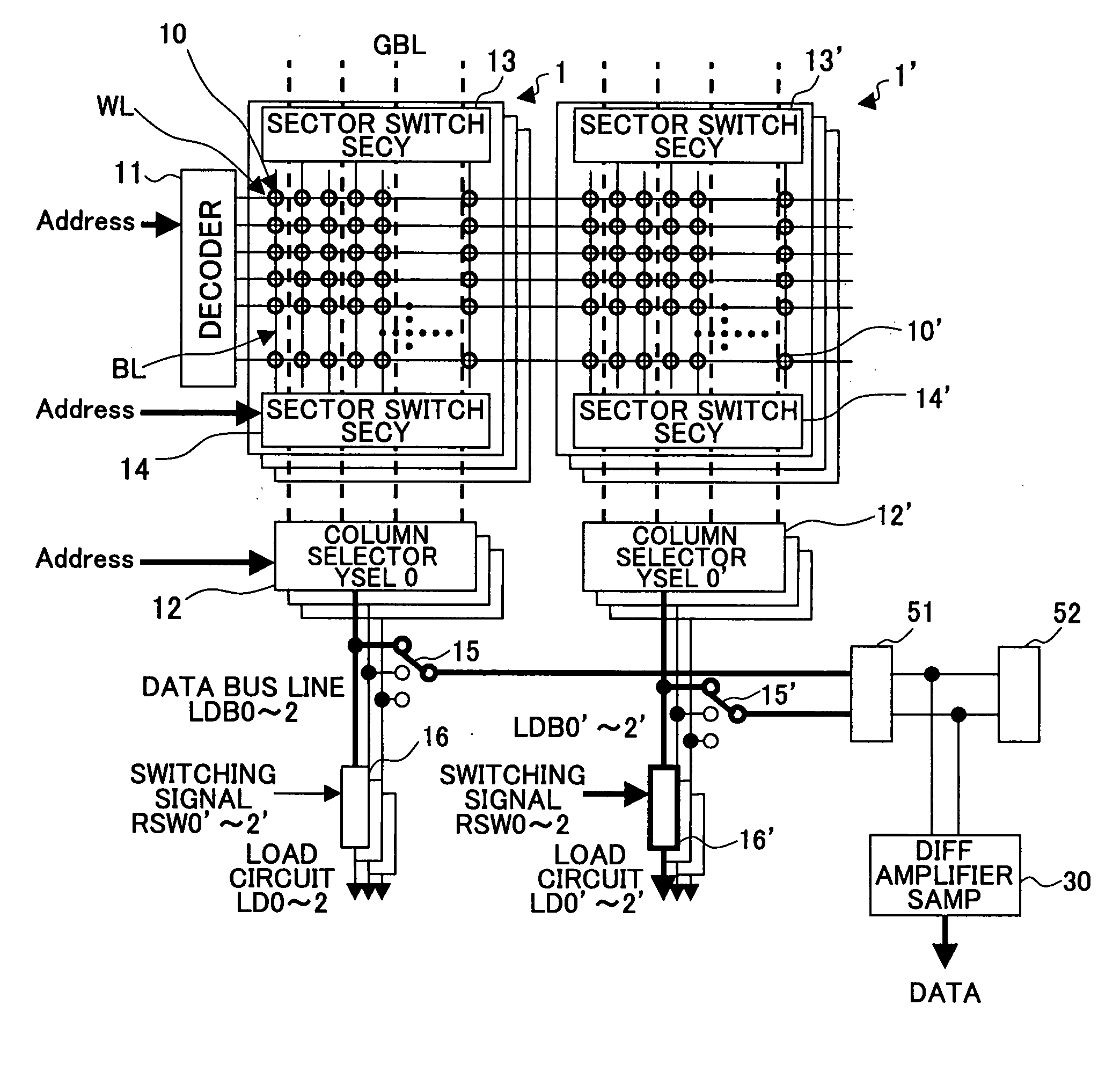
[0050]FIG. 5 shows the composition of the read-out circuit of the nonvolatile semiconductor memory device in the first preferred embodiment of the invention. In the nonvolatile semiconductor memory device of FIG. 5, each memory cell holds the four-level data, similar to the composition of FIG. 2.

[0051] The nonvolatile semiconductor memory device of FIG. 5 comprises the first memory core portion 1, the second memory core portion 1′ having the memory cell arrangement that is the same as that of the first memory core portion 1, and the read-out circuit.

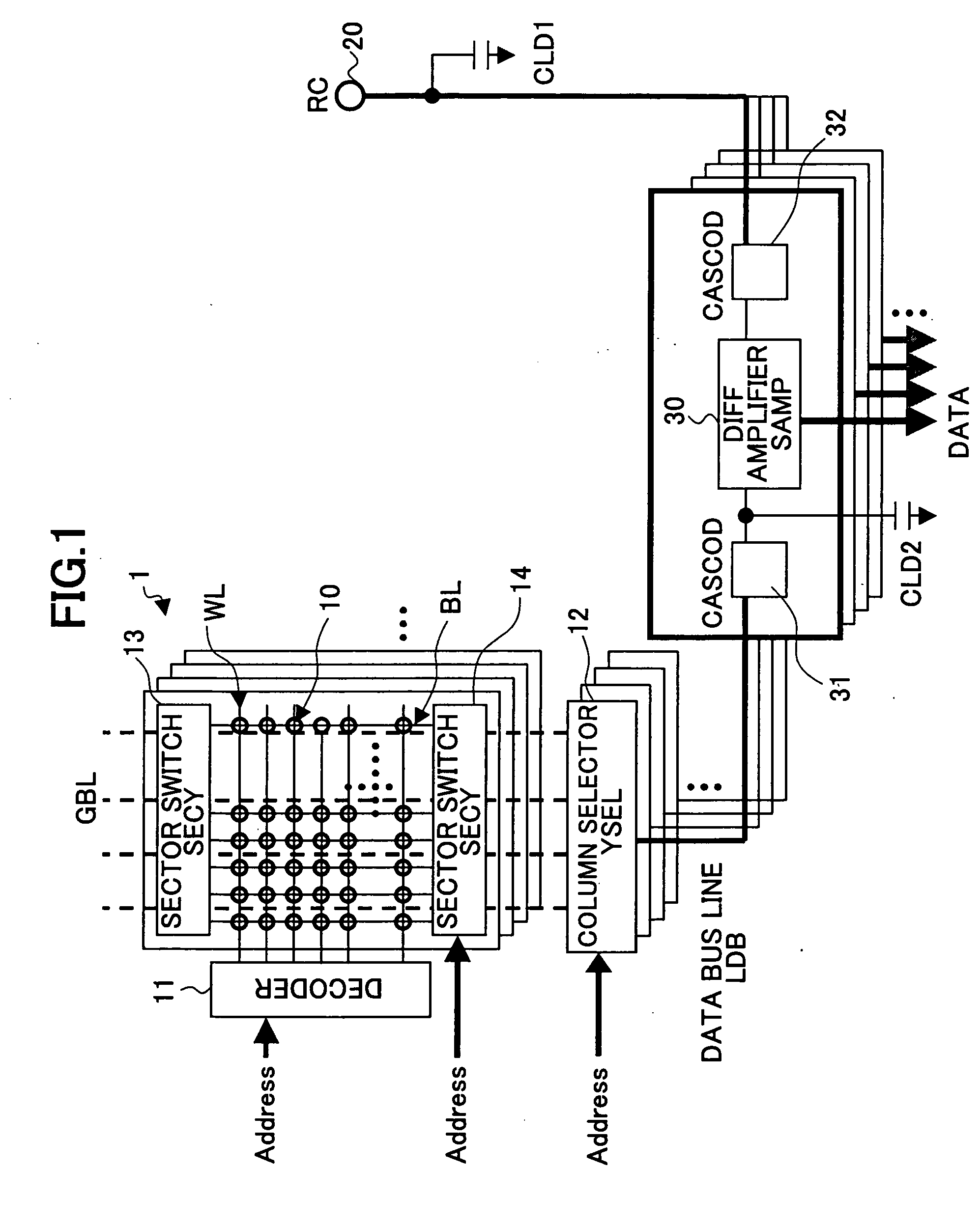
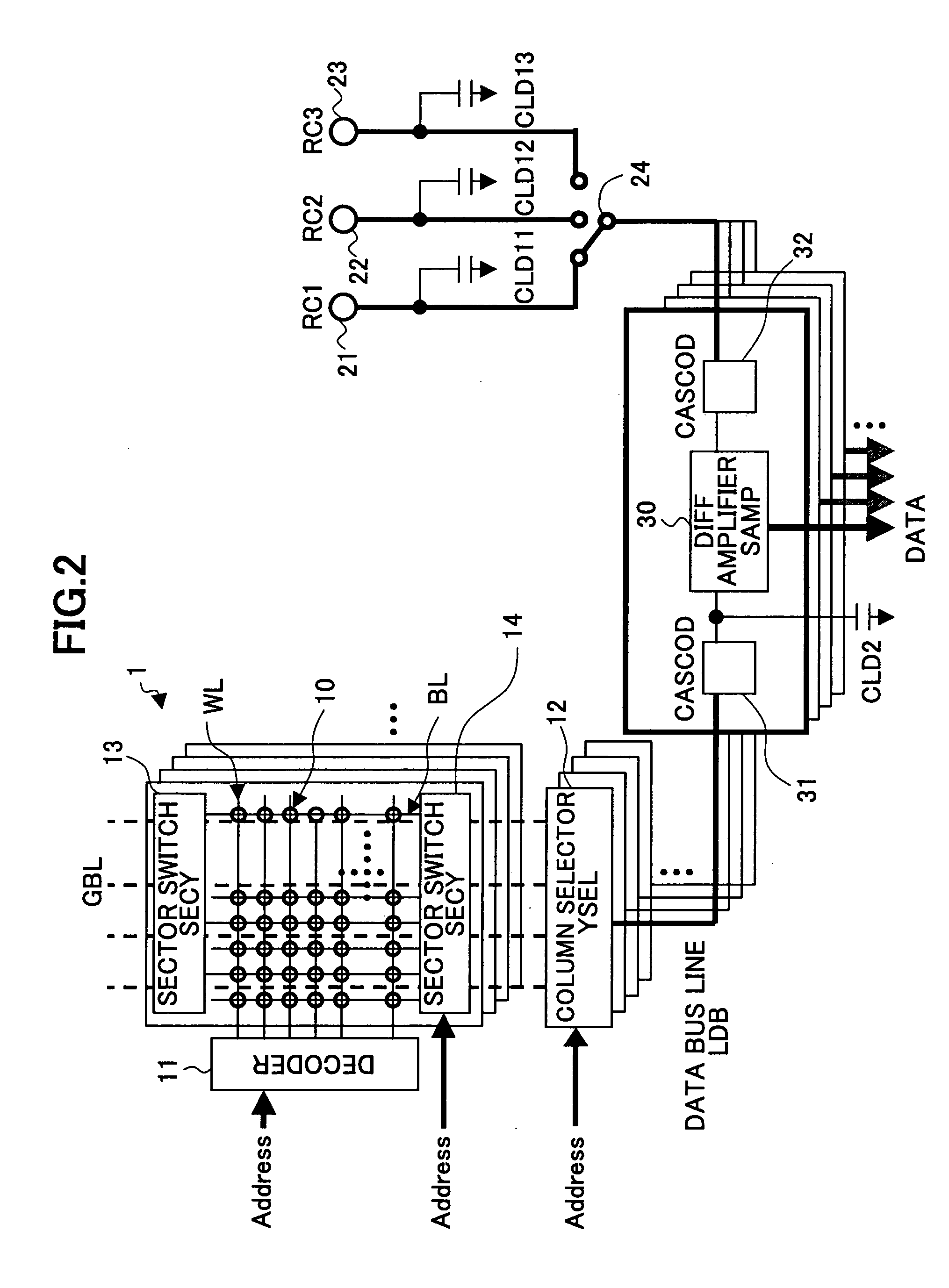
[0052] The first memory core portion 1 comprises the plurality of nonvolatile memory cells 10 (first memory cell array) which are connected in the 2-dimensional matrix formation by the word lines WL and the bit lines BL, the decoder 11 to which the address signal is inputted, the column selector (YSEL) 12, t...


PUM


Abstract

A nonvolatile semiconductor memory device comprises a memory cell array in which memory cells each holding memory cell information are arrayed, reference cells which supply different reference currents respectively, and a read-out circuit. When reading the memory cell information from a selected one of the memory cells, the read-out circuit is brought into conduction to a first global bit line which is connected to a bit line of the selected memory cell, and brought into conduction to one of a plurality of second global bit lines respectively which are provided near the first global bit line and connected to bit lines of non-selected memory cells but not connected to the bit line of the selected memory cell, so that the memory cell information is determined by comparing a read-out current from the selected memory cell with each of the reference currents from the reference cells.

Description

CROSS-REFERENCE TO RELATED APPLICATION [0001] This application is a U.S. continuation application which is filed under 35 USC 111(a) and claims the benefit under 35 USC 120 and 365(c) of International Application No. PCT / JP2003 / 02514, filed on Mar. 4, 2003, the entire contents of which are hereby incorporated by reference.BACKGROUND OF THE INVENTION [0002] 1. Field of the Invention [0003] The present invention generally relates to a reading operation of reading the memory cell information in a nonvolatile semiconductor memory device, and more particularly to a nonvolatile semiconductor memory device provided with a read-out circuit for reading the multi-level information held in the memory cells at high speed. [0004] 2. Description of the Related Art [0005] In a nonvolatile semiconductor memory device, such as a flash memory, memory cell information is stored by using the current drive capacity of the nonvolatile transistor in the nonvolatile memory cell. That is, the memory cell in...

Claims


Application Information

Patent Timeline
IPC IPC(8): G11C7/14G11C16/26G11C16/28
CPCG11C7/14G11C2207/002G11C16/28
Inventor IKEDA, TOSHIMIHATAKEYAMA, ATSUSHITANIGUCHI, NOBUTAKAKIKUTAKE, AKIRAKAWABATA, KUNINORITAKEUCHI, ATSUSHI
Owner SOCIONEXT INC
Why Eureka
Try Eureka