Light emitting diode

a diode and light-emitting technology, applied in the field of light-emitting diodes, can solve the problems of inability to adapt to back-light sources and the growing demand for smaller thicknesses, and achieve the effect of reducing thickness and high efficiency

Active Publication Date: 2005-08-04
CITIZEN ELECTRONICS CO LTD
View PDF2 Cites 95 Cited by
  • Summary
  • Abstract
  • Description
  • Claims
  • Application Information

AI Technical Summary

Benefits of technology

[0008] An object of this invention is to provide a side emission type light emitting diode (LED) that can be reduced in thickness...

Problems solved by technology

However, because of its construction of FIG. 12, in which the LED chip 4 is mounted on the die bond pattern 7 provided on the side of the chip substrate 2 and is enclosed by and sealed with the light transmitting resin body 5, the LED 1, though it can be reduced in thickness, has the light from the LED chip 4 scattered and therefore is not suited...

Method used


Image

  • Light emitting diode
  • Light emitting diode
  • Light emitting diode

Examples


first embodiment

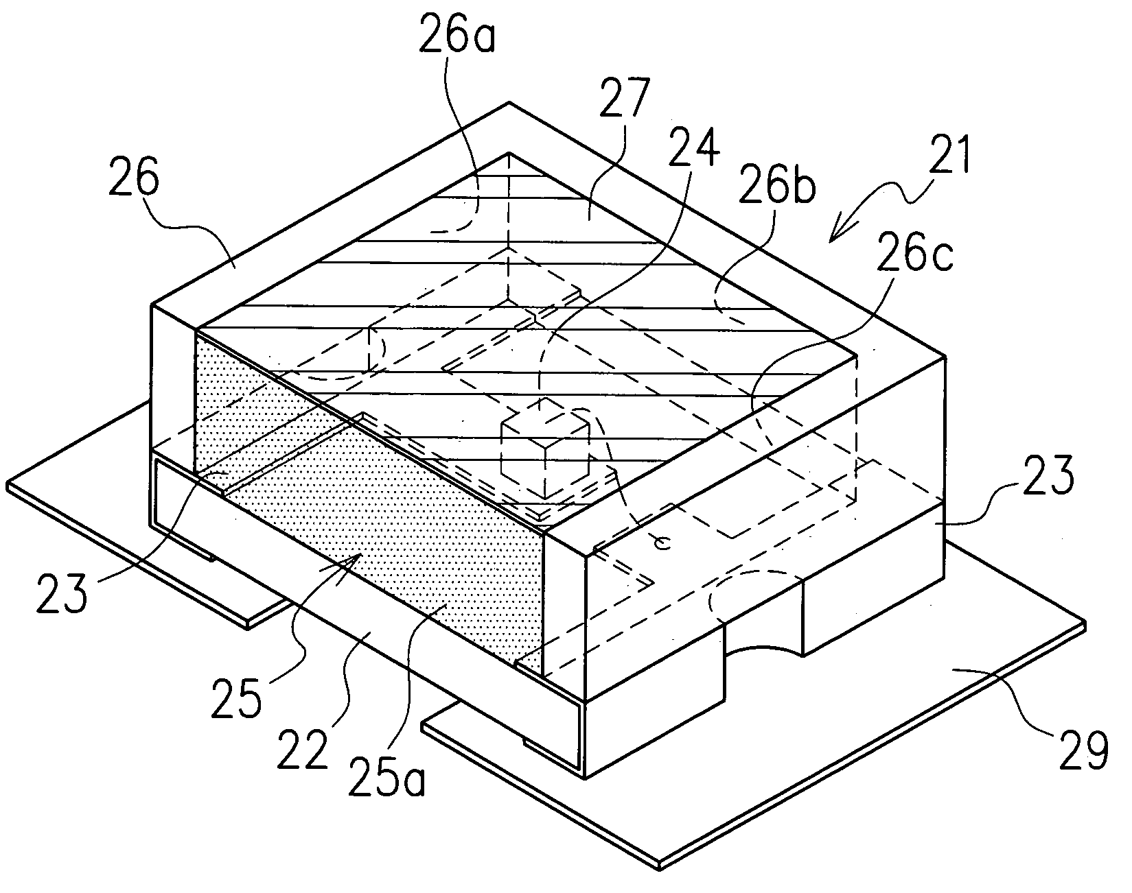
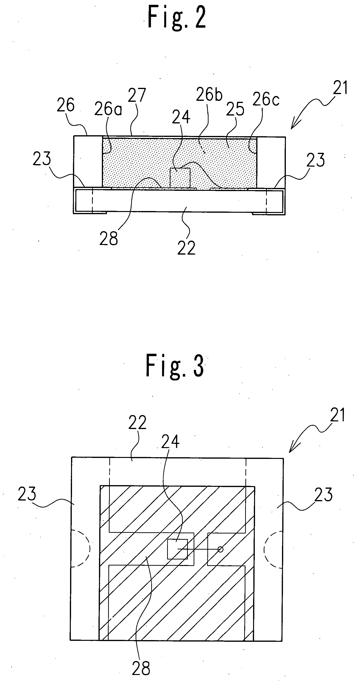
[0026]FIG. 1 is a perspective view of the LED of the invention; FIG. 2 is a cross-sectional view of the LED shown in FIG. 1; and FIG. 3 is a plan view of the LED shown in FIG. 1.

[0027] As shown in FIG. 1 to FIG. 3, the LED 21 of this invention comprises an LED chip 24 mounted on a chip substrate 22 formed by glass epoxy or BT resin (bismaleimide triazine resin), a light transmissive resin body 25 that seals the LED chip 24 on the chip substrate 22, a reflective frame 26 enclosing the light transmissive resin body 25 on three sides, and a reflective film 27 formed over the light transmissive resin body 25. On its three inner sides the reflective frame 26 has reflecting surfaces 26a, 26b, 26c so that light from the LED chip 24 is directed toward a resin surface (light emission face 25a) of the light transmissive resin body 25 which is not enclosed by the reflecting surfaces 26a, 26b, 26c and the reflective film 27.

[0028] The chip substrate 22 is provided with electrode terminals 23 t...

fifth embodiment

[0038]FIG. 10 and FIG. 11 illustrate an LED 61 according to this invention. This LED 61 has a blue LED chip 64a, a green LED chip 64b and a red LED chip 64c and can emit light of multiple colors. These LED chips are mounted side by side on a chip substrate 62 which has three sets of paired electrode terminals 63, each made up of anode and cathode. They are sealed with a light transmissive resin body 65. The light transmissive resin body 65 is enclosed by a reflective frame 66 on its three sides and provided with a reflective film 67 on its upper surface.

[0039] The arrangement of the LED chips is as follows. As shown in FIG. 10 and FIG. 11, the red LED chip 64c is put at the deepest position in a space enclosed by the reflective frame 66, with the green LED chip 64b and the blue LED chip 64aarranged toward a light emission face 65a in that order. As described above, by placing the near-transparent LED chips, such as green and blue LED chips 64b, 64a, closer to the light emission face...


PUM


Abstract

An LED comprises: a chip substrate formed with a die bond pattern and electrode terminals; an LED chip mounted on the chip substrate; a reflective frame arranged on the chip substrate to enclose a circumference of the LED chip and having an opening at a part of its side walls and on an upper surface; reflecting surfaces formed on inner circumferential surfaces of the side walls of the reflective frame; a light transmissive resin body formed in the reflective frame and using the opening in the side wall as a light emission face; and a reflecting film covering an upper surface of the light transmissive resin body exposed on an upper surface side of the reflective frame; wherein light produced by the LED chip is reflected by a reflecting surface of the refractive frame and by the reflecting film and is emitted outward from the light emission face. The side emission type LED of this construction can be reduced in thickness for surface mounting and can illuminate a small-width side surface of a liquid crystal panel with high efficiency.

Description

CROSS REFERENCE TO RELATED APPLICATION [0001] The application claims the priority benefit of Japanese Patent Application No. 2004-28325, filed on Feb. 4, 2004, the entire description of which is incorporated herein by reference. BACKGROUND OF THE INVENTION [0002] 1. Field of the Invention [0003] The present invention relates to a light emitting diode (LED) of a side emission type that illuminates a thin display body such as a liquid crystal panel from its side. [0004] 2. Description of Related Art [0005] As a backlight source to illuminate a display panel such as a liquid crystal display from its side, an LED of a side emission type such as disclosed in Japanese Patent Disclosure No. 2002-368281 has been known. This LED 1, as shown in FIG. 12, comprises a chip substrate 2 formed with a die bond pattern 7 and electrode terminals 3, an LED chip 4 mounted on the die bond pattern 7, and a light transmitting resin body 5 that seals the LED chip 4. An LED 11 shown in FIG. 13 is made by ha...

Claims


Application Information

Patent Timeline
IPC IPC(8): G02B6/00H01L27/15H01L33/46H01L33/50H01L33/60H01L33/62
CPCH01L33/54H01L33/60H01L2224/48091H01L2924/00014
Inventor FUKASAWA, KOICHI
Owner CITIZEN ELECTRONICS CO LTD
Why Eureka
Try Eureka