Methods and structures for electronic probing arrays

a technology of electronic probe arrays and methods, applied in the direction of electronic circuit testing, measurement devices, instruments, etc., can solve the problems of probe cards, potential to harm chip contacts, non-uniform forces between the tips of the probe contacts and the wafer contacts

Inactive Publication Date: 2005-08-04
TESSERA INC
View PDF15 Cites 18 Cited by
  • Summary
  • Abstract
  • Description
  • Claims
  • Application Information

AI Technical Summary

Problems solved by technology

This typically leads to non-uniform forces between the tips of the probe contacts and the wafer contacts.
If too much force is placed on any one probe contact, there is a potential to harm the chip contacts.
The typical failure mode of such a probe card is the absence of the probe contacts uniformly engaging the end surfaces of the chip contacts.
These circumstances result in a number of inherent problems during the probing process as described hereinabove.

Method used


Image

  • Methods and structures for electronic probing arrays
  • Methods and structures for electronic probing arrays
  • Methods and structures for electronic probing arrays

Examples


Embodiment Construction

[0019] In describing the preferred embodiments of the invention illustrated in the drawings, specific terminology will be used for the sake of clarity. However, the invention is not intended to be limited to the specific terms so selected, and it is to be understood that each specific term includes all technical equivalents that operate in a similar manner to accomplish a similar purpose.

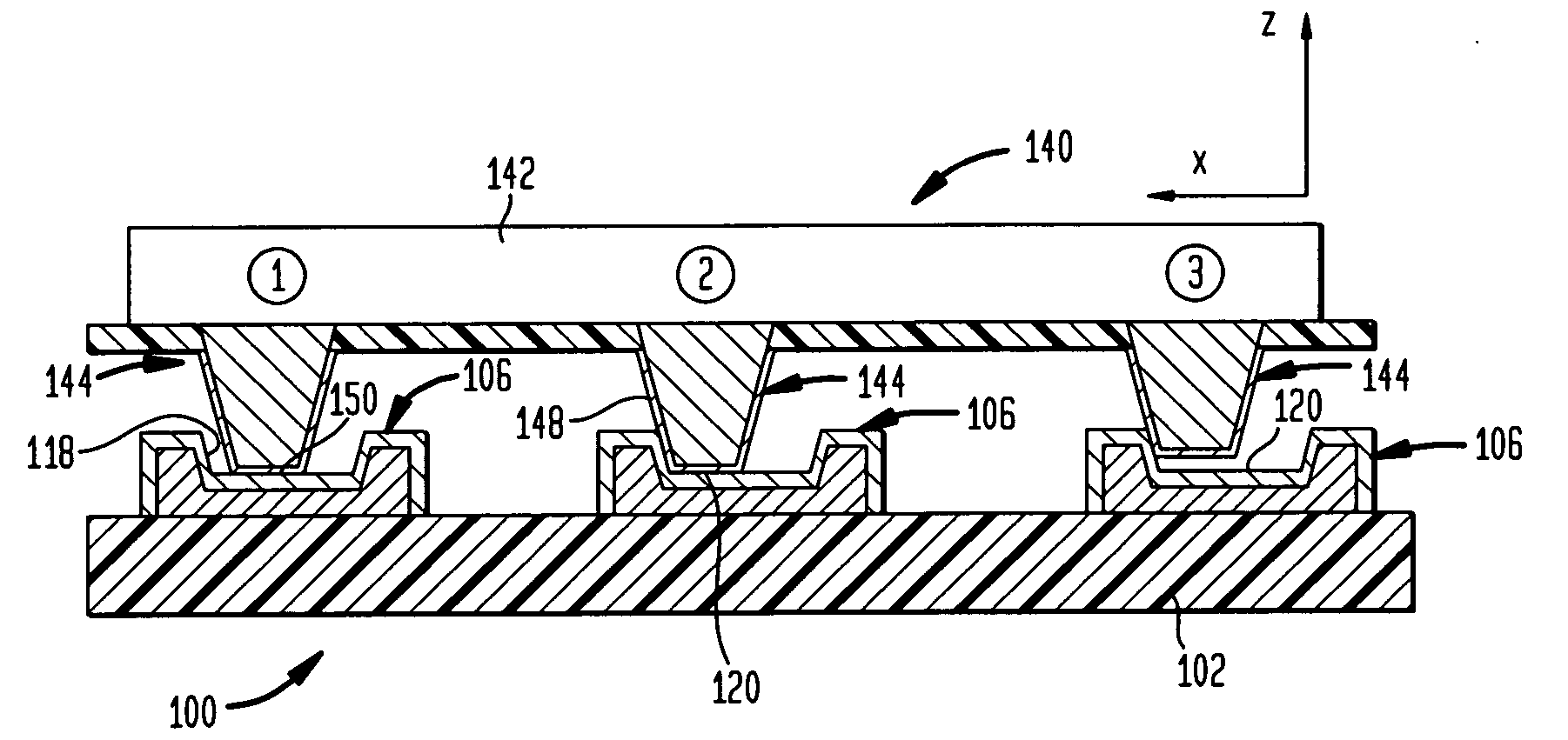
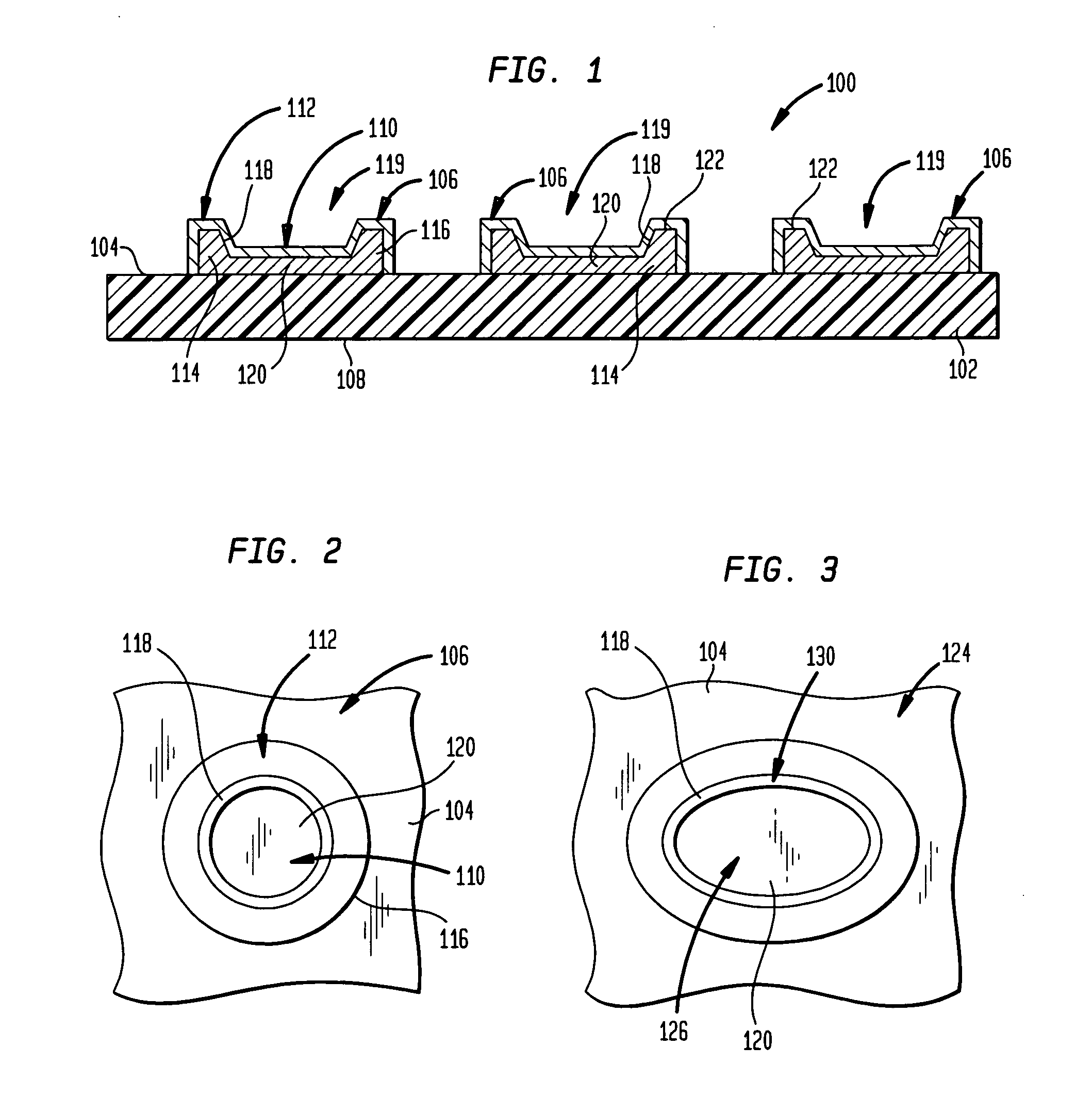
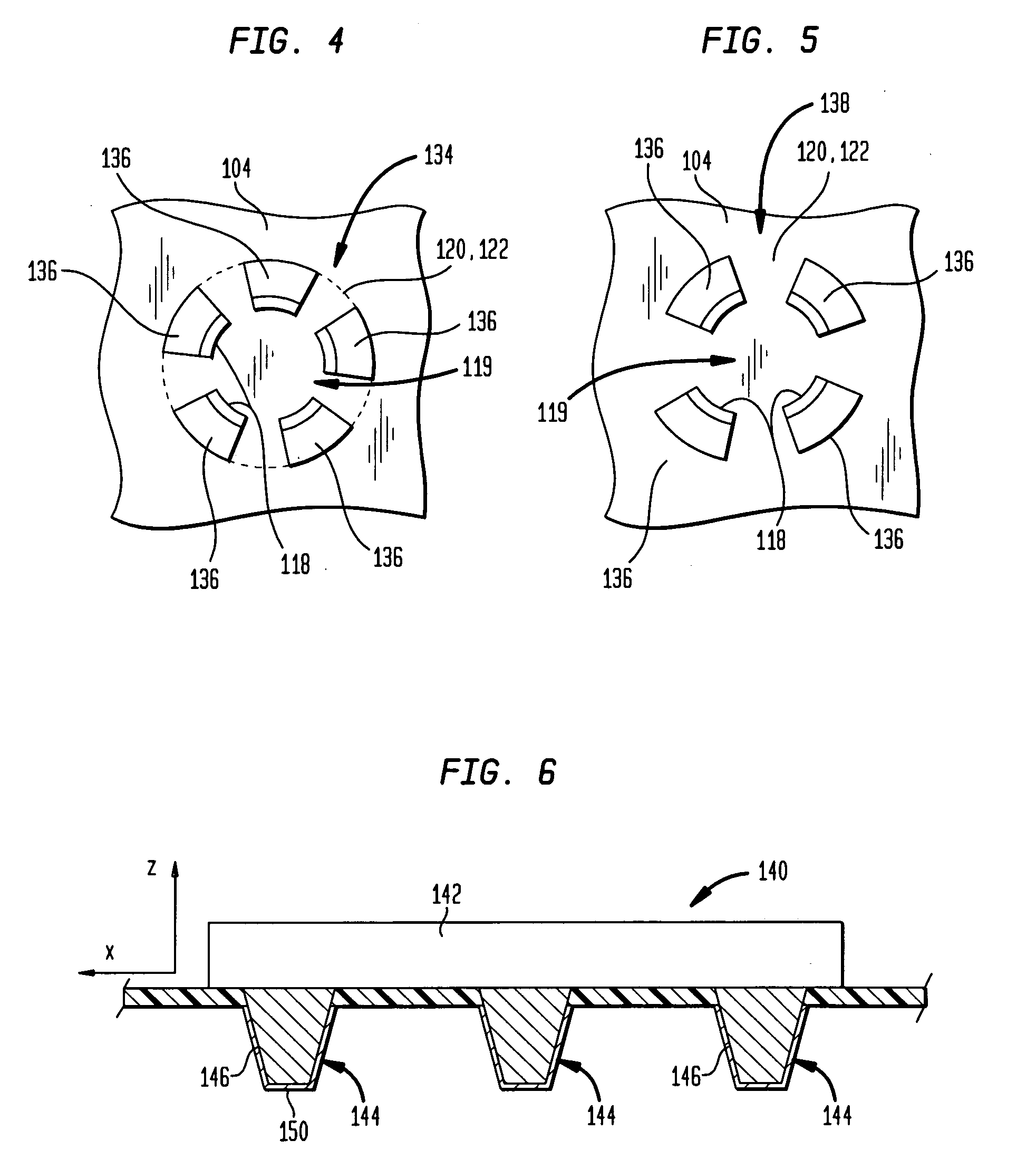
[0020] Turning to the drawings, wherein like reference numeral represent like elements, there is shown in FIG. 1 a testing probe constructed in accordance with an embodiment of the present invention generally designated by reference numeral 100. The probe 100 includes a substrate 102 having a planar upper surface 104 supporting a plurality of probe contacts 106 and a bottom surface 108. The substrate 102, in accordance with a preferred embodiment, is formed from a rigid dielectric polymer material such as polyimide. It is to be understood that other polymeric materials may be used for the substrate...


PUM


Abstract

A probe for testing semiconductor chips includes a plurality of probe contacts providing z-direction compliancy. The probe contacts include a blind opening surrounded by a lateral sidewall for receiving an aligned chip contact. The chip contacts are manipulated with a downward vertical force and along a horizontal path for engagement with various portions of the probe contact within the blind opening. The alignment may be actively monitored for determining minimum contact resistance during the probing process.

Description

CROSS REFERENCES TO RELATED APPLICATIONS [0001] This application claims the benefit of the filing date of U.S. Provisional Patent Application No. 60 / 532,706 filed on Dec. 24, 2003, the disclosure of which is hereby incorporated herein by reference.BACKGROUND OF THE INVENTION [0002] Semiconductor chips are typically manufactured en masse in so called wafers. Each wafer is made of a semiconductor material and typically is four to twelve inches in diameter. Each wafer typically contains a plurality of identical chips each connected and adjacent one another, but separated by portions of the wafer called scribe lines. The scribe lines do not contain devices which are required in the finished chips. Generally, the individual chips are separated (or “diced”) from one another for packaging and / or electrical connection to other chips. Prior to the further processing and connection, however, the chips are desirably tested in order to determine which chips are defective so that further expense...

Claims


Application Information

Patent Timeline
Patent Type & Authority Applications(United States)
IPC IPC(8): G01R31/28
CPCG01R31/2887
Inventor KIM, YOUNG-GON
Owner TESSERA INC
Why Eureka
Try Eureka