Devices and methods for side-coupling optical fibers to optoelectronic components

a technology of optical fiber and optoelectronic components, applied in the field of optical devices, can solve the problems of increasing light loss, affecting the coupling effect of light, and being unacceptable for various applications, so as to maximize the coupling effect and minimize the distance between the optical fiber cor

Inactive Publication Date: 2005-08-04
INT BUSINESS MASCH CORP
View PDF31 Cites 22 Cited by
  • Summary
  • Abstract
  • Description
  • Claims
  • Application Information

AI Technical Summary

Benefits of technology

[0026] It is an object of the invention to minimize the distance between an optical fiber core and an optical component (e.g., optoelectronic device (or array), imaging device, light guiding device, etc.) when side-coupling light so as to maximize the coupling of light to and from the fiber or fiber array to the optical component.
[0027] It is another object of the invention to provide a modified silicon V-groove channel (or array of modified silicon V-groove channels) for mounting an optical fiber(s), which allow a precisely controlled portion of the cladding layer to be removed using a substrate surface as a polishing stop, so that the separation between the fiber core(s) and an optical component (e.g., optoelectronic device), which is side-coupled thereto, can be reduced resulting in improved optical coupling.
[0038] In another aspect of the invention, an optical connector comprises a substrate comprising a first array of recessed v-groove channels in a first portion of the substrate and a second array of recessed v-groove channels in a second portion of the substrate. Each recessed v-groove channel in the first and second arrays is inclined relative to the surface of the substrate, and each recessed v-groove in the first array is axially aligned with a recessed v-groove in the second array. A fiber optic cable is mounted in the substrate, wherein a buffer polymer portion of the fiber optic cable with optical fibers comprising a core, cladding layer and buffer layer are mounted in the recessed v-groove channels in the second portion of the substrate, and wherein optical fibers comprising a fiber core and cladding layer, which extend from the buffer polymer portion of the fiber optic cable, are mounted in the recessed v-groove channels of the first portion of the substrate. A portion of the cladding layer and buffer layer of the optical fibers extending beyond the surface of the substrate are polished substantially planar with the surface of the substrate. This optical connector can be directly side-coupled to an optical component (e.g., a substrate comprising an array of optoelectronic devices), and the inclined recessed v-groove channels having optical fibers mounted therein provide adequate stress relief to prevent breakage of the fibers.

Problems solved by technology

This method requires a large spacing between PCBs because of the large minimum bending radius of the optical fibers and results in increased light loss, which may not be acceptable for various applications.
The light-coupling systems and methods described in the above patents all suffer from the disadvantages described below.
One disadvantage is that the closest possible spacing between the optoelectronic device 5 and the center of the optical fiber 1 is limited by the radius of the optical fiber 1, including both the core 2 and cladding layer 3.
Another disadvantage is that unless an index matching material is used, light being coupled out from the fiber 1 to a photodetector is spread-out more in the direction parallel to the fiber axis 6 than perpendicular to the fiber.
This-results in asymmetric divergence which makes it difficult to use further optics to focus the light.
This large spot size will not be acceptable for future high speed optical communications systems where lower optical coupling losses are needed.
This leads to a significant problem because if an array of fibers held by silicon V-groove substrates is being joined to another assembly which does not transmit UV light, it is difficult or impossible to properly expose and cure the UV glue forming the join if the layer is thin, such as less than 5-10 microns.
Additionally, for a connector which uses alignment pins, it can be difficult to see the cavity into which the guide pins go from above when bring the v-groove blocks together.

Method used


Image

  • Devices and methods for side-coupling optical fibers to optoelectronic components
  • Devices and methods for side-coupling optical fibers to optoelectronic components
  • Devices and methods for side-coupling optical fibers to optoelectronic components

Examples


Embodiment Construction

. PREFERRED EMBODIMENTS

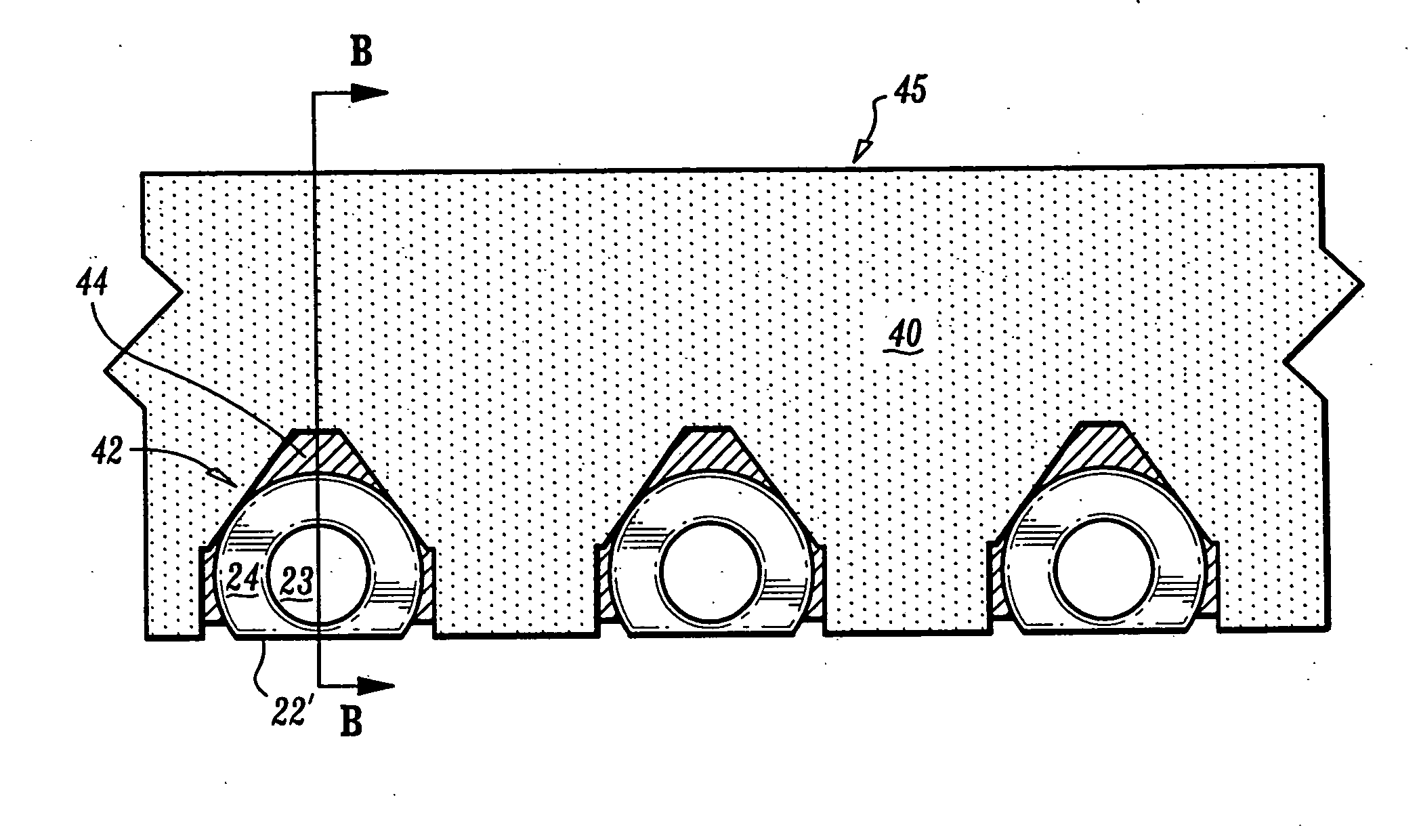
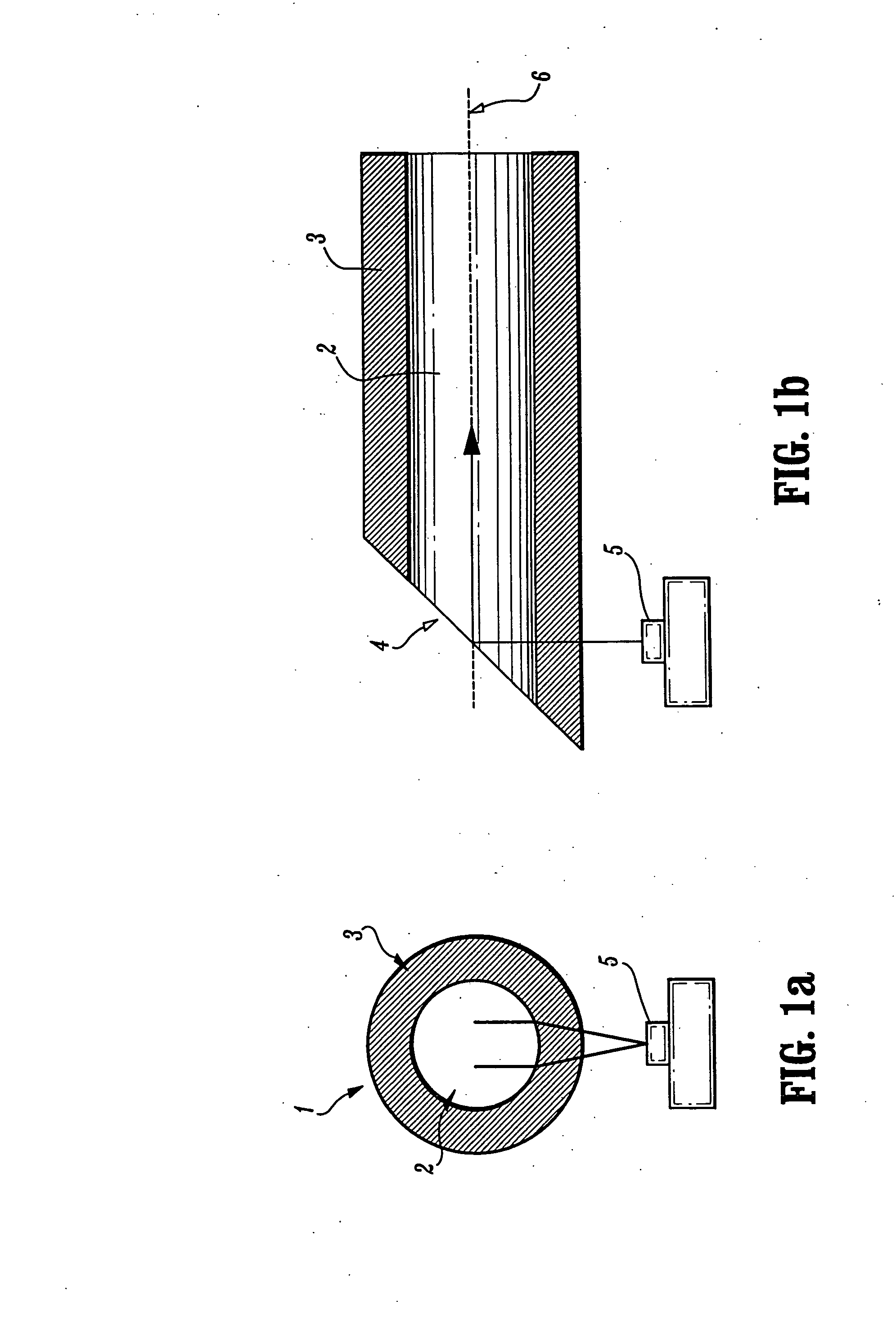
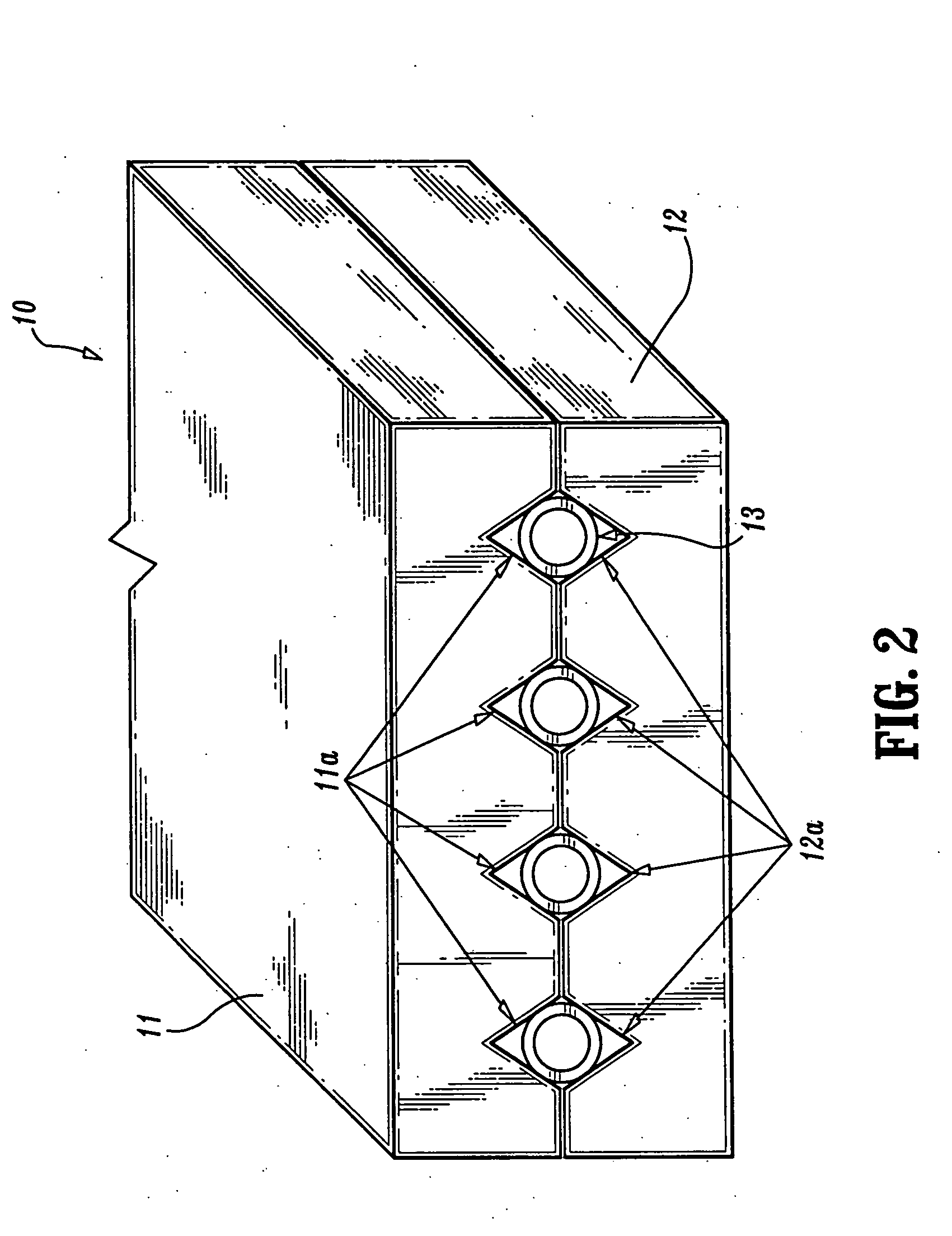
[0050] The present invention is directed to optical devices, components and methods for mounting optical fibers and for side-coupling light to / from optical fibers using a modified silicon V-groove, or silicon V-groove array, wherein V-grooves (for precisely aligning / spacing optical fibers) are “recessed” below the surface of the silicon. Methods according to the invention for forming recessed silicon V-grooves or v-groove arrays, enable optical fibers to be recessed below the surface of the silicon substrate such, that a precisely controlled portion of the cladding layer extending above the silicon surface can be removed (lapped) using the surface of the silicon as a polishing stop. With the cladding layer removed, the separation between the fiber core(s) and the optoelectronic device(s) is reduced, resulting in improved optical coupling when the optical fiber silicon array is connected to an optoelectronic device array, e.g., a VCSEL array.

[0051] More specif...


PUM

PropertyMeasurementUnit
diameteraaaaaaaaaa
diameteraaaaaaaaaa
diameteraaaaaaaaaa

Abstract

Optical devices, components and methods for mounting optical fibers and for side-coupling light to / from optical fibers using a modified silicon V-groove, or silicon V-groove array, wherein V-grooves, which are designed for precisely aligning / spacing optical fibers, are “recessed” below the surface of the silicon. Optical fibers can be recessed below the surface of the silicon substrate such that a precisely controlled portion of the cladding layer extending above the silicon surface can be removed (lapped). With the cladding layer removed, the separation between the fiber core(s) and optoelectronic device(s) can be reduced resulting in improved optical coupling when the optical fiber silicon array is connected to, e.g., a VCSEL array.

Description

TECHNICAL FIELD OF THE INVENTION [0001] The present invention is generally related to optical devices and methods for manufacturing optical devices. More specifically, the invention relates to devices and methods for side-coupling optoelectronic components (e.g., semiconductor light sources, detectors), or other optical devices (e.g., wave guides) to optical transmission lines (e.g., optical fibers) that are mounted in recessed V-groove channels formed in a silicon substrate. BACKGROUND [0002] The development of small, efficient optical transmission lines such as optical fibers, has lead to widespread use of optical communication in many applications requiring, e.g., long distance, high data rate communication such as telecommunications. Optical fibers typically include a transparent core surrounded by a transparent cladding material having a refractive index lower than that of the core. Further, optical fibers (core and cladding) are typically coated with a polymer buffer layer, wh...

Claims


Application Information

Patent Timeline
Patent Type & Authority Applications(United States)
IPC IPC(8): G02B6/36G02B6/42
CPCG02B6/3636G02B6/3652G02B6/423G02B6/4214G02B6/3692
Inventor COLGAN, EVAN GEORGEDOANY, FUAD ELIASFURMAN, BRUCE KENNETHSTIGLIANI, DANIEL J. JR.
Owner INT BUSINESS MASCH CORP
Why Eureka
Try Eureka