Integrated circuit device and fabrication method therefor
a technology of integrated circuits and fabrication methods, applied in solid-state devices, thin film varistors, basic electric elements, etc., to achieve the effect of simplifying the fabrication process of integrated circuit devices and reducing restrictions on etching conditions
- Summary
- Abstract
- Description
- Claims
- Application Information
AI Technical Summary
Benefits of technology
Problems solved by technology
Method used
Image
Examples
second embodiment
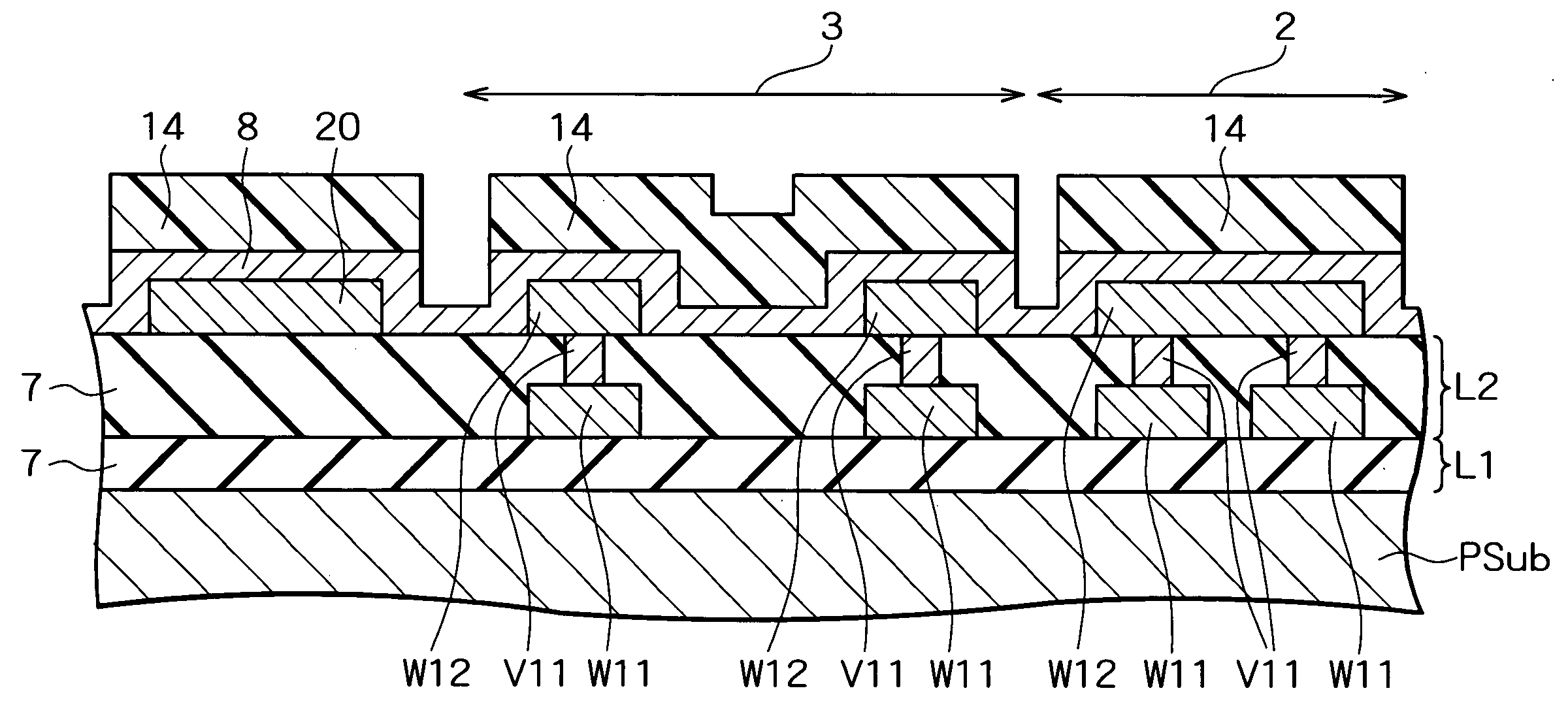
[0058] the present invention will be discussed below. FIG. 5 is a cross-sectional view showing a semiconductor integrated circuit device according to the present embodiment. As shown in FIG. 5, in the present embodiment, a vanadium oxide layer 8 is also provided at the region of a semiconductor integrated circuit device 6 which is other than the temperature sensor section 3, e.g., at the logic circuit section 2, in such a way as to cover the top and side surfaces of the wires W12. The top and side surfaces of the periphery of the external pad 20 are likewise covered with the vanadium oxide layer 8.
first embodiment
[0059] The opening 19 is formed in such a way as to penetrate the vanadium oxide layer 8 and reach the external pad 20. Therefore, the top center portion of the external pad 20 is not covered with the vanadium oxide layer 8, and is exposed at the bottom of the opening 19. The vanadium oxide layer 8 is provided at the same level and with the same thickness as the temperature monitor element 10. The other structure of the present embodiment is the same as that of the
third embodiment
[0060] the present invention will be discussed below. FIG. 6 is a cross-sectional view showing a semiconductor integrated circuit device according to the present embodiment. As shown in FIG. 6, in the present embodiment, an insulating layer 11 is provided at the wiring layer L3 in a semiconductor integrated circuit device 9 in such a way as to cover the wires W12. Vias 12 are formed at a part of the region of the insulating layer 11 which directly lies above the wires W12 in the temperature sensor section 3. A part of the temperature monitor element 10 is buried in the vias 12. Accordingly, the temperature monitor element 10 is connected to the wires W12 in the vias 12.
[0061] The opening 19 is formed in such a way as to penetrate the insulating layer 11 and reach the external pad 20. Therefore, the top center portion of the external pad 20 is not covered with the insulating layer 11, and is exposed at the bottom of the opening 19. The other structure of the embodiment is the same as...
PUM
 Abstract
Description
Claims
Application Information


