Display panel and method for manufacturing display panel

Inactive Publication Date: 2005-08-11
SANYO ELECTRIC CO LTD
View PDF4 Cites 13 Cited by
  • Summary
  • Abstract
  • Description
  • Claims
  • Application Information

AI Technical Summary

Benefits of technology

[0010] According to the present invention, a pixel substrate and a sealing substrate are joined through sealing by welding using laser irradiation. Therefore, sealing can be reliably achieved with a small area and an area of a display region in which the display can be actually realized can be increased. As a consequence, the size of the display can be reduced. In addition, because the joining is achieved by welding, it is possible to reliably prevent moisture from intruding and to reduce the amount of desiccant to be sealed inside or to omit such a desiccant. Moreover, because a region of the absorbing structure to be used in the welding can be limited to a portion in w

Problems solved by technology

In the method of using the nontransparent glass, however, the e

Method used


Image

  • Display panel and method for manufacturing display panel
  • Display panel and method for manufacturing display panel
  • Display panel and method for manufacturing display panel

Examples


Embodiment Construction

[0022] A preferred embodiment (hereinafter, referred to simply as “embodiment”) of the present invention will now be described referring to the drawings.

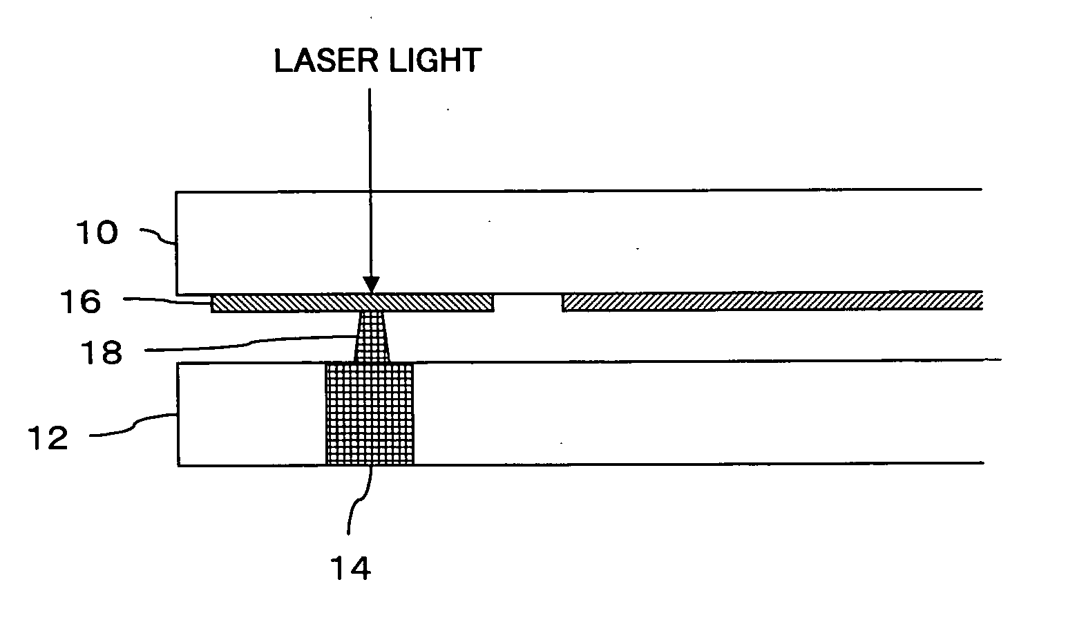
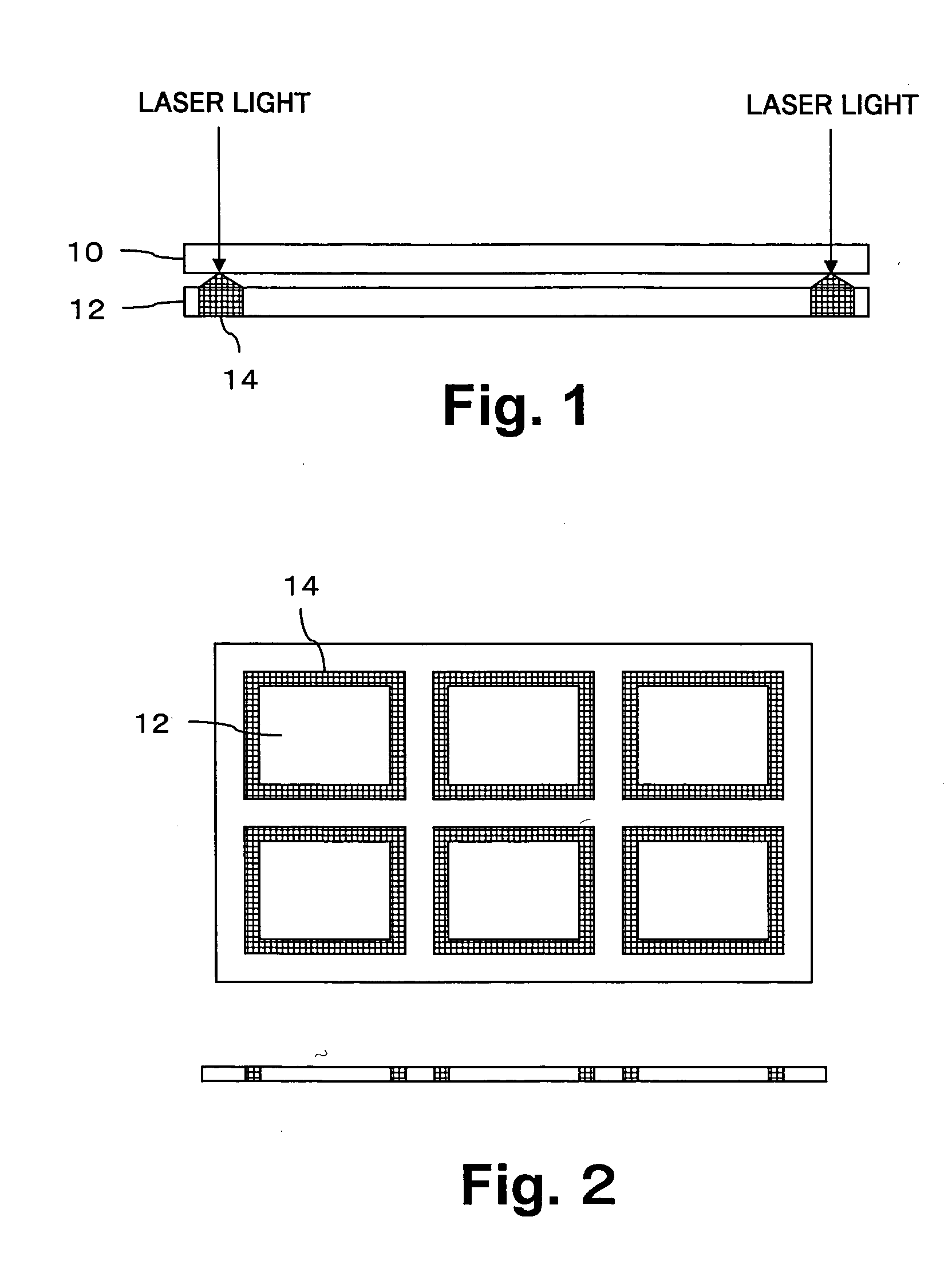
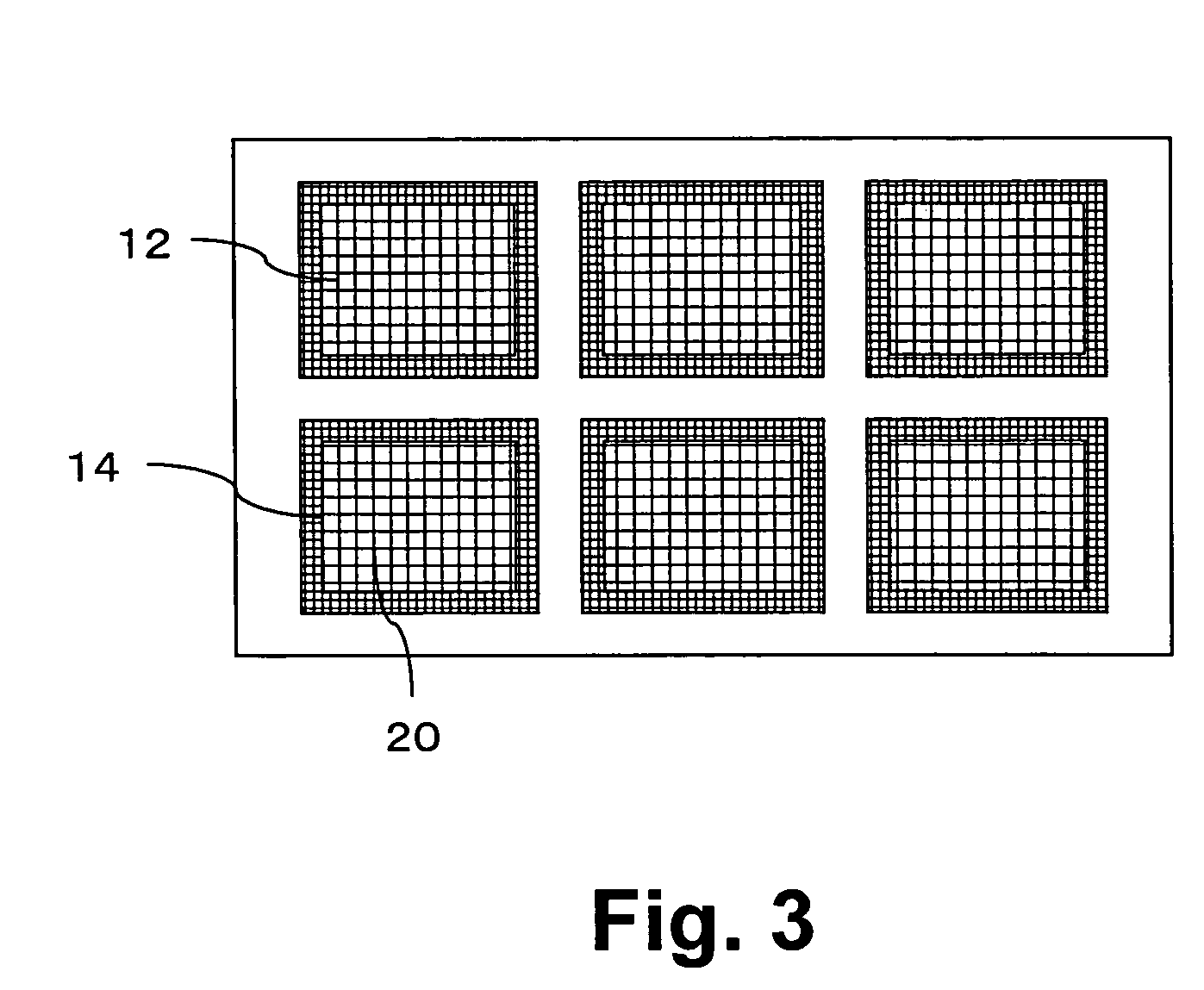
[0023]FIGS. 1 and 2 show joining of substrates according to a preferred embodiment of the present invention. An EL substrate 10 which is a pixel substrate on which a pixel or pixels are formed and a sealing substrate 12 for sealing an upper surface of the EL substrate 10 are placed opposing each other. The sealing substrate 12 has an absorbing structure region which absorbs laser such as a nontransparent glass in the portion to be sealed by welding. For example, the sealing substrate 12 can be made nontransparent by doping a metal though an ion injection or ion exchange method, for example, and a nontransparent region 14 which functions as an absorbing structure region which absorbs laser light is formed. In the ion exchange method, a resist which is patterned so as to expose the portion to become a nontransparent region is formed ...


PUM


Abstract

A sealing substrate and an EL substrate are placed opposing each other with a predetermined gap therebetween. A nontransparent region is formed in a peripheral portion of the sealing substrate in advance. The nontransparent region is irradiated with laser through the EL substrate so that the nontransparent region is heated and glass is elevated and welded. Because portions of the sealing substrate other than the nontransparent region are clear, it is possible to realize a top emission type structure.

Description

CROSS-REFERENCE TO RELATED APPLICATIONS [0001] The entire disclosure of Japanese Patent Application No. 2004-12457 including specification, claims, drawings and abstract is incorporated herein by reference. BACKGROUND OF THE INVENTION [0002] 1. Field of the Invention [0003] The present invention relates to manufacture of a display panel such as an organic electroluminescence (hereinafter simply referred to as “EL”) display panel and, in particular, to a sealing structure in the display panel. [0004] 2. Description of the Related Art [0005] Plasma display panels (PDP) and liquid crystal display devices (LCD) are becoming widely available as thin flat display panels and organic EL panels are commercially available. [0006] In an organic EL panel, an organic material is used as a light emitting material in each pixel or the like. Because the lifetime of the organic material is shortened when the organic material contains moisture, it is necessary to minimize an amount of moisture in a s...

Claims


Application Information

Patent Timeline
IPC IPC(8): G09F9/00H01J1/62H05B33/04H01J9/26H01L27/32H01L51/50H01L51/52H01L51/56H05B33/10H05B33/12H05B33/14
CPCH01J9/261H01L27/3244H01L2251/5315H01L51/56H01L51/5237H10K59/12H10K50/8426H10K2102/3026H10K71/00F21V17/12
Inventor NISHIKAWA, RYUJIOMURA, TETSUJI
Owner SANYO ELECTRIC CO LTD
Why Eureka
Try Eureka